|
|
PDF TDF8541 Data sheet ( Hoja de datos )
| Número de pieza | TDF8541 | |
| Descripción | I2C-bus controlled 4 x 45 W power amplifier | |
| Fabricantes | NXP Semiconductors | |
| Logotipo | ||
Hay una vista previa y un enlace de descarga de TDF8541 (archivo pdf) en la parte inferior de esta página. Total 30 Páginas | ||
|
No Preview Available !
TDF8541
I2C-bus controlled 4 45 W power amplifier
Rev. 3 — 13 December 2011
Product data sheet
1. General description
The TDF8541 is one of a new generation of complementary quad Bridge-Tied Load (BTL)
audio power amplifiers intended for automotive applications. It has full I2C-bus controlled
diagnostics, including start-up diagnostics. The TDF8541 can operate at a battery voltage
as low as 6 V making this amplifier suitable for stop/start-car operation.
The amplifier uses a complementary DMOS output stage in a Silicon-On-Insulator (SOI)-
based BCD process. The DMOS output stage ensures a high power output signal with
perfect sound quality. The SOI-based BCD process ensures a robust amplifier, where
latch-up cannot occur, with good separation between the four independent channels, with
every component isolated and without substrate currents.
2. Features and benefits
Stop/start-car prepared: keeps operating without audible disturbance during engine
start at a battery voltage as low as 6 V
Operates in either legacy (non I2C-bus) or I2C-bus modes (3.3 V and 5 V compliant)
Four hardware-programmable I2C-bus addresses
Can drive 2 and 4 loads
Speaker fault detection
Start-up diagnostics with load detection: open, short, present; filtered for door-slam
and chatter relays
AC load (tweeter) detection with low and high current mode
Gain select after start-up without audible disturbance
Independent selectable soft mute of front and rear channels
Programmable gain (26 dB and 16 dB), independently programmable for the front and
rear channels
Line driver mode supports engine start at a battery voltage as low as 6 V (16 dB and
mid-tap voltage 0.25VP)
Programmable clip detect: 2 %, 5 % or 10 %
Programmable thermal pre-warning
Pin STB can be programmed/multiplexed with second-clip detect
Clip information of each channel can be directed separately to pin DIAG or pin STB
Independent enabling of thermal- , clip- or load fault information (short across the load
or to VP or to ground) on pin DIAG
Loss-of-ground and open VP safe (minimum series resistance required)
All amplifier outputs short-circuit proof to ground, supply voltage and across the load
(channel independent)
All pins short-circuit proof to ground
1 page 
NXP Semiconductors
TDF8541
I2C-bus controlled 4 45 W power amplifier
TAB 36
n.c. 35
n.c. 34
n.c. 33
PGND3 32
n.c. 31
ACGND 30
IN3 29
IN4 28
SGND 27
IN2 26
IN1 25
SVR 24
PGND1 23
n.c. 22
n.c. 21
n.c. 20
n.c. 19
TDF8541TH
1 OUT3-
2 OUT3+
3 VP1
4 OUT4-
5 PGND4
6 OUT4+
7 SCL
8 SDA
9 DIAG
10 ADSEL
11 STB
12 n.c.
13 OUT2+
14 PGND2
15 OUT2-
16 VP2
17 OUT1+
18 OUT1-
001aan085
Fig 3. Pin configuration of type TDF8541TH (package HSOP36)
TDF8541
Product data sheet
All information provided in this document is subject to legal disclaimers.
Rev. 3 — 13 December 2011
© NXP B.V. 2011. All rights reserved.
5 of 54
5 Page 
NXP Semiconductors
TDF8541
I2C-bus controlled 4 45 W power amplifier
switched off. If several channels have a short across the load at the same time, the
channels are switched on one by one to prevent high supply current switching with four
shorts across the load at the same time. The 15 ms cycle reduces power dissipation. To
prevent audible distortion, the channel with the short can be disabled via the I2C-bus.
7.4.2
Loss-of-ground/loss of VP
Loss-of-ground/loss of VP is a double fault condition: the ground (or VP) wire of the set is
not connected and the ground (or VP) wire is connected to one of the loudspeaker
outputs. In this situation the supply capacitor in the set is charged through the body diode
of the output power transistor. This body diode (between the drain and source of the
power transistor) is always present in amplifiers with MOS output stages. The capacitor
charge current depends on the series impedance of the supply lines, the output
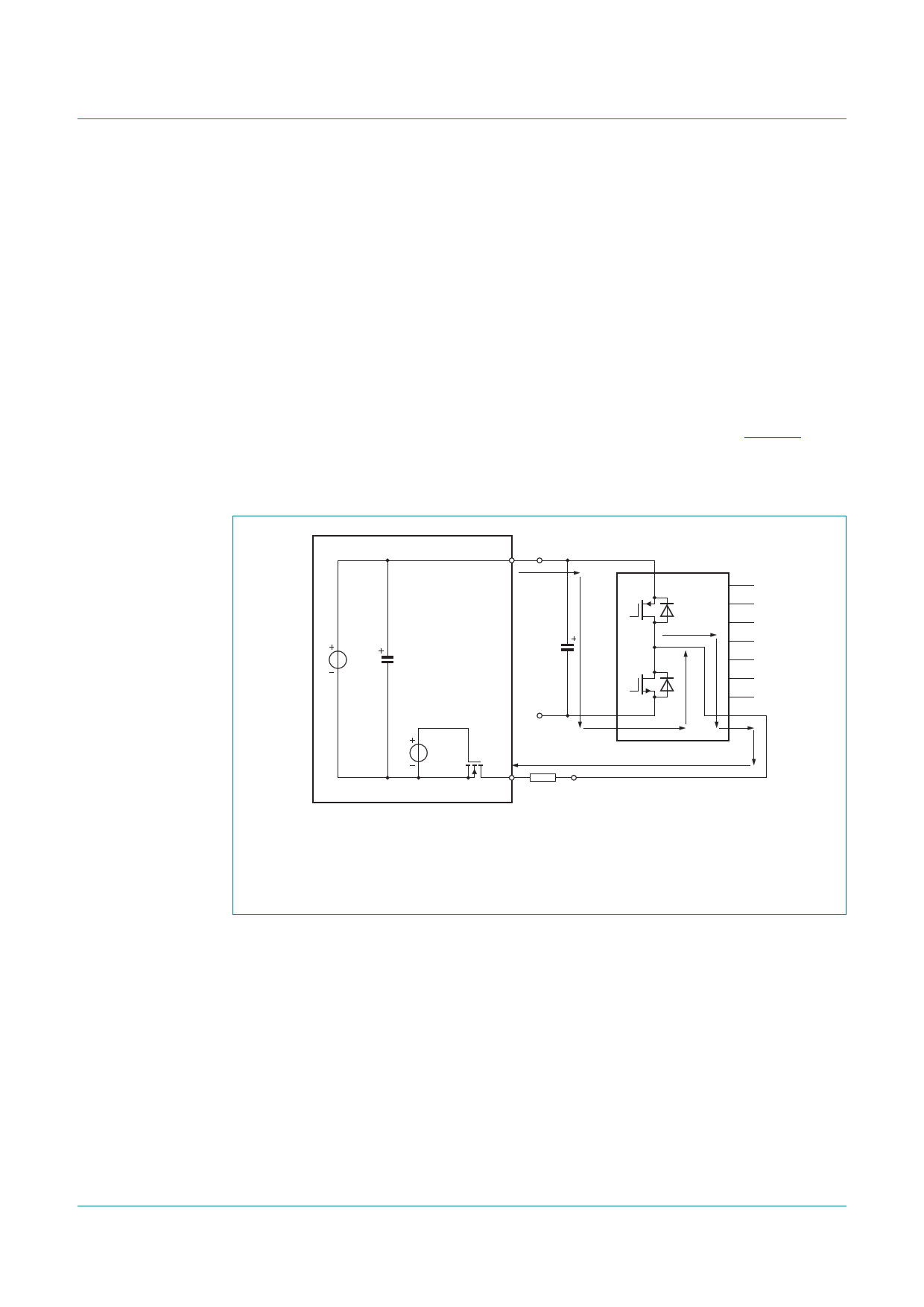
impedance of the loss-of-ground tester and the value of the capacitor; see Figure 7. To
simulate a worst-case condition, the loss-of-ground tester is equipped with a buffer
capacitor of 116 mF to simulate a very low output impedance. With a RS of 63 m, peak
currents of more than 70 A have been measured.
VP
Cbuffer
116 mF
(1)
2200 μF
NMOS
Vpulse 80N03L
Loss-of-ground tester
RS
(1) Capacitor can be 2200 F to 10000 F.
(2) Amplifier output stage.
Fig 7. Test circuit for loss-of-ground test
(2) 3
5
7
9
17
19
21
23
DUT in application
001aam695
TDF8541
Product data sheet
All information provided in this document is subject to legal disclaimers.
Rev. 3 — 13 December 2011
© NXP B.V. 2011. All rights reserved.
11 of 54
11 Page | ||
| Páginas | Total 30 Páginas | |
| PDF Descargar | [ Datasheet TDF8541.PDF ] | |
Hoja de datos destacado
| Número de pieza | Descripción | Fabricantes |
| TDF8541 | I2C-bus controlled 4 x 45 W power amplifier | NXP Semiconductors |
| TDF8546 | 4 x 45 W best efficiency amplifier | NXP Semiconductors |
| Número de pieza | Descripción | Fabricantes |
| SLA6805M | High Voltage 3 phase Motor Driver IC. |
Sanken |
| SDC1742 | 12- and 14-Bit Hybrid Synchro / Resolver-to-Digital Converters. |
Analog Devices |
|
DataSheet.es es una pagina web que funciona como un repositorio de manuales o hoja de datos de muchos de los productos más populares, |
| DataSheet.es | 2020 | Privacy Policy | Contacto | Buscar |
