|
|
|
PDF HIP6601A Data sheet ( Hoja de datos )
| Número de pieza | HIP6601A | |
| Descripción | Synchronous Rectified Buck MOSFET Drivers | |
| Fabricantes | Intersil Corporation | |
| Logotipo | ||
Hay una vista previa y un enlace de descarga de HIP6601A (archivo pdf) en la parte inferior de esta página. Total 11 Páginas | ||
|
No Preview Available !
RECOMMEONBHD®SIEPOD6L6RE0ET1PEBDL,aPAHtRaCIPOES6DMh6U0eEC3eNBtTT PRODUCT
HIP6601A, HIP6603A, HIP6604
August 2004
FN4884.5
Synchronous Rectified Buck MOSFET
Drivers
The HIP6601A, HIP6603A and HIP6604 are high frequency,
dual MOSFET drivers specifically designed to drive two
power N-Channel MOSFETs in a synchronous rectified buck
converter topology. These drivers combined with a HIP63xx
or an ISL65xx Multi-Phase Buck PWM controller form a
complete core-voltage regulator solution for advanced
microprocessors.
The HIP6601A drives the lower gate in a synchronous
rectifier to 12V, while the upper gate can be independently
driven over a range from 5V to 12V. The HIP6603A drives
both upper and lower gates over a range of 5V to 12V. This
drive-voltage flexibility provides the advantage of optimizing
applications involving trade-offs between switching losses
and conduction losses. The HIP6604 can be configured as
either a HIP6601A or a HIP6603A.
The output drivers in the HIP6601A, HIP6603A and HIP6604
have the capacity to efficiently switch power MOSFETs at
frequencies up to 2MHz. Each driver is capable of driving a
3000pF load with a 30ns propagation delay and 50ns
transition time. These products implement bootstrapping on
the upper gate with only an external capacitor required. This
reduces implementation complexity and allows the use of
higher performance, cost effective, N-Channel MOSFETs.
Adaptive shoot-through protection is integrated to prevent
both MOSFETs from conducting simultaneously.
Ordering Information
TEMP. RANGE
PART NUMBER (oC) PACKAGE
PKG.
DWG. #
HIP6601ACB
0 to 85
8 Ld SOIC M8.15
HIP6603ACB
0 to 85
8 Ld SOIC M8.15
HIP6601ACB-T 8 Ld SOIC Tape and Reel
HIP6603ACB-T 8 Ld SOIC Tape and Reel
HIP6601ECB
0 to 85
8 Ld EPSOIC M8.15B
HIP6603ECB
0 to 85
8 Ld EPSOIC M8.15B
HIP6601ECB-T 8 Ld EPSOIC Tape and Reel
HIP6603ECB-T
HIP6604CR
HIP6604CR-T
8 Ld EPSOIC Tape and Reel
0 to 85
16 Ld 4x4 QFN L16.4x4
16 Ld 4x4 QFN Tape and Reel
Features
• Drives Two N-Channel MOSFETs
• Adaptive Shoot-Through Protection
• Internal Bootstrap Device
• Supports High Switching Frequency
- Fast Output Rise Time
- Propagation Delay 30ns
• Small 8 Lead SOIC and EPSOIC and 16 Lead QFN
Packages
• Dual Gate-Drive Voltages for Optimal Efficiency
• Three-State Input for Output Stage Shutdown
• Supply Under Voltage Protection
Applications
• Core Voltage Supplies for Intel Pentium® III, AMD®
Athlon™ Microprocessors
• High Frequency Low Profile DC-DC Converters
• High Current Low Voltage DC-DC Converters
Related Literature
• Technical Brief TB363 “Guidelines for Handling and
Processing Moisture Sensitive Surface Mount Devices
(SMDs)”
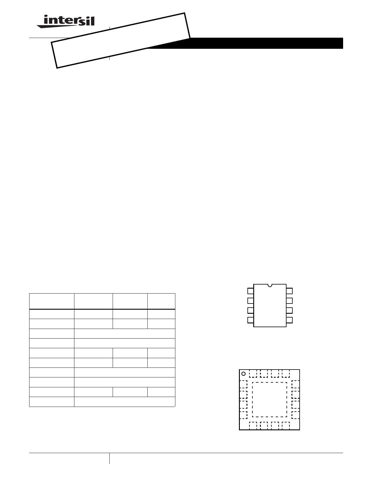
Pinouts
HIP6601ACB, HIP6603ACB (SOIC)
HIP6601ECB, HIP6603ECB (EPSOIC)
TOP VIEW
UGATE 1
BOOT 2
PWM 3
GND 4
8 PHASE
7 PVCC
6 VCC
5 LGATE
HIP6604 (QFN)
TOP VIEW
16 15 14 13
NC 1
BOOT 2
PWM 3
GND 4
12 NC
11 PVCC
10 LVCC
9 VCC
5678
1 CAUTION: These devices are sensitive to electrostatic discharge; follow proper IC Handling Procedures.
1-888-INTERSIL or 321-724-7143 | Intersil (and design) is a registered trademark of Intersil Americas Inc.
Copyright © Intersil Americas Inc. 2003, 2004. All Rights Reserved.
All other trademarks mentioned are the property of their respective owners.
1 page 
HIP6601A, HIP6603A, HIP6604
Functional Pin Description
UGATE (Pin 1), (Pin 16 QFN)
Upper gate drive output. Connect to gate of high-side power
N-Channel MOSFET.
BOOT (Pin 2), (Pin 2 QFN)
Floating bootstrap supply pin for the upper gate drive.
Connect the bootstrap capacitor between this pin and the
PHASE pin. The bootstrap capacitor provides the charge to
turn on the upper MOSFET. A resistor in series with boot
capacitor is required in certain applications to reduce ringing
on the BOOT pin. See the Internal Bootstrap Device section
under DESCRIPTION for guidance in choosing the
appropriate capacitor and resistor values.
PWM (Pin 3), (Pin 3 QFN)
The PWM signal is the control input for the driver. The PWM
signal can enter three distinct states during operation, see the
three-state PWM Input section under DESCRIPTION for further
details. Connect this pin to the PWM output of the controller.
GND (Pin 4), (Pin 4 QFN)
Bias and reference ground. All signals are referenced to this
node.
PGND (Pin 5 QFN Package Only)
This pin is the power ground return for the lower gate driver.
LGATE (Pin 5), (Pin 7 QFN)
Lower gate drive output. Connect to gate of the low-side
power N-Channel MOSFET.
VCC (Pin 6), (Pin 9 QFN)
Connect this pin to a +12V bias supply. Place a high quality
bypass capacitor from this pin to GND.
LVCC (Pin 10 QFN Package Only)
Lower gate driver supply voltage.
Timing Diagram
PVCC (Pin 7), (Pin 11 QFN)
For the HIP6601A and the HIP6604, this pin supplies the
upper gate drive bias. Connect this pin from +12V down to
+5V.
For the HIP6603A, this pin supplies both the upper and
lower gate drive bias. Connect this pin to either +12V or +5V.
PHASE (Pin 8), (Pin 14 QFN)
Connect this pin to the source of the upper MOSFET and the
drain of the lower MOSFET. The PHASE voltage is
monitored for adaptive shoot-through protection. This pin
also provides a return path for the upper gate drive.
Description
Operation
Designed for versatility and speed, the HIP6601A, HIP6603A
and HIP6604 dual MOSFET drivers control both high-side and
low-side N-Channel FETs from one externally provided PWM
signal.
The upper and lower gates are held low until the driver is
initialized. Once the VCC voltage surpasses the VCC Rising
Threshold (See Electrical Specifications), the PWM signal
takes control of gate transitions. A rising edge on PWM
initiates the turn-off of the lower MOSFET (see Timing
Diagram). After a short propagation delay [tPDLLGATE], the
lower gate begins to fall. Typical fall times [tFLGATE] are
provided in the Electrical Specifications section. Adaptive
shoot-through circuitry monitors the LGATE voltage and
determines the upper gate delay time [tPDHUGATE] based
on how quickly the LGATE voltage drops below 2.2V. This
prevents both the lower and upper MOSFETs from
conducting simultaneously or shoot-through. Once this delay
period is complete the upper gate drive begins to rise
[tRUGATE] and the upper MOSFET turns on.
PWM
tPDHUGATE
tRUGATE
tPDLUGATE
tFUGATE
UGATE
LGATE
tPDLLGATE
tFLGATE
5
tPDHLGATE
tRLGATE
5 Page 
HIP6601A, HIP6603A, HIP6604
Small Outline Plastic Packages (SOIC)
N
INDEX
AREA
E
-B-
H
0.25(0.010) M B M
123
-A-
D
SEATING PLANE
A
L
h x 45o
-C-
e A1
B
0.25(0.010) M C A M B S
µα
0.10(0.004)
C
NOTES:
1. Symbols are defined in the “MO Series Symbol List” in Section 2.2 of
Publication Number 95.
2. Dimensioning and tolerancing per ANSI Y14.5M-1982.
3. Dimension “D” does not include mold flash, protrusions or gate burrs.
Mold flash, protrusion and gate burrs shall not exceed 0.15mm (0.006
inch) per side.
4. Dimension “E” does not include interlead flash or protrusions. Inter-
lead flash and protrusions shall not exceed 0.25mm (0.010 inch) per
side.
5. The chamfer on the body is optional. If it is not present, a visual index
feature must be located within the crosshatched area.
6. “L” is the length of terminal for soldering to a substrate.
7. “N” is the number of terminal positions.
8. Terminal numbers are shown for reference only.
9. The lead width “B”, as measured 0.36mm (0.014 inch) or greater
above the seating plane, shall not exceed a maximum value of
0.61mm (0.024 inch).
10. Controlling dimension: MILLIMETER. Converted inch dimensions
are not necessarily exact.
M8.15 (JEDEC MS-012-AA ISSUE C)
8 LEAD NARROW BODY SMALL OUTLINE PLASTIC
PACKAGE
INCHES
MILLIMETERS
SYMBOL MIN MAX MIN MAX NOTES
A
0.0532 0.0688 1.35
1.75
-
A1
0.0040 0.0098 0.10
0.25
-
B
0.013 0.020 0.33
0.51
9
C
0.0075 0.0098 0.19
0.25
-
D
0.1890 0.1968 4.80
5.00
3
E
0.1497 0.1574 3.80
4.00
4
e 0.050 BSC 1.27 BSC -
H
0.2284 0.2440 5.80
6.20
-
h
0.0099 0.0196 0.25
0.50
5
L
0.016 0.050 0.40
1.27
6
N8
87
α 0o 8o 0o 8o -
Rev. 0 12/93
All Intersil products are manufactured, assembled and tested utilizing ISO9000 quality systems.
Intersil Corporation’s quality certifications can be viewed at website www.intersil.com/design/quality
Intersil products are sold by description only. Intersil Corporation reserves the right to make changes in circuit design and/or specifications at any time without notice.
Accordingly, the reader is cautioned to verify that data sheets are current before placing orders. Information furnished by Intersil is believed to be accurate and reliable. How-
ever, no responsibility is assumed by Intersil or its subsidiaries for its use; nor for any infringements of patents or other rights of third parties which may result from its use.
No license is granted by implication or otherwise under any patent or patent rights of Intersil or its subsidiaries.
For information regarding Intersil Corporation and its products, see web site www.intersil.com
11
11 Page | ||
| Páginas | Total 11 Páginas | |
| PDF Descargar | [ Datasheet HIP6601A.PDF ] | |
Hoja de datos destacado
| Número de pieza | Descripción | Fabricantes |
| HIP6601 | Synchronous-Rectified Buck MOSFET Drivers | Intersil Corporation |
| HIP6601A | Synchronous Rectified Buck MOSFET Drivers | Intersil Corporation |
| HIP6601B | (HIP6601B / HIP6603B / HIP6604B) Synchronous Rectified Buck MOSFET Drivers | Intersil Corporation |
| HIP6601CB | Synchronous-Rectified Buck MOSFET Drivers | Intersil Corporation |
| Número de pieza | Descripción | Fabricantes |
| SLA6805M | High Voltage 3 phase Motor Driver IC. |
Sanken |
| SDC1742 | 12- and 14-Bit Hybrid Synchro / Resolver-to-Digital Converters. |
Analog Devices |
|
DataSheet.es es una pagina web que funciona como un repositorio de manuales o hoja de datos de muchos de los productos más populares, |
| DataSheet.es | 2020 | Privacy Policy | Contacto | Buscar |