|
|
|
PDF CH7006C-T Data sheet ( Hoja de datos )
| Número de pieza | CH7006C-T | |
| Descripción | Digital PC to TV Encoder Features | |
| Fabricantes | ETC | |
| Logotipo | ||
Hay una vista previa y un enlace de descarga de CH7006C-T (archivo pdf) en la parte inferior de esta página. Total 30 Páginas | ||
|
No Preview Available !
CHRONTEL
CH7006C
Digital PC to TV Encoder Features
Features
• Function compatible with CH7004
• Universal digital interface accepts YCrCb (CCIR601
or 656) or RGB (15, 16 or 24-bit) video data in both
non-interlaced and interlaced formats
• TrueScale TM rendering engine supports underscan
operations for various graphic resolutions† ¥
• Enhanced text sharpness and adaptive flicker removal
with up to 5-lines of filtering†
• Enhanced dot crawl control and area reduction
• Fully programmable through I2C port
• Supports NTSC, NTSC-EIA (Japan), and PAL (B, D,
G, H, I, M and N) TV formats
• Provides Composite, S-Video and SCART outputs
• Auto-detection of TV presence
• Supports VBI pass-through
• Programmable power management
• 9-bit video DAC outputs
• Complete Windows and DOS driver software
• Offered in 44-pin PLCC, 44-pin TQFP
† Patent number 5,781,241
¥ Patent number 5,914,753
General Description
Chrontel’s CH7006 digital PC to TV encoder is a stand-
alone integrated circuit which provides a PC 99 compliant
solution for TV output. Suggested application use with the
Intel I740.* It provides a universal digital input port to
accept a pixel data stream from a compatible VGA
controller (or equivalent) and converts this directly into
NTSC or PAL TV format.
This circuit integrates a digital NTSC/PAL encoder with
9-bit DAC interface, and new adaptive flicker filter, and
high accuracy low-jitter phase locked loop to create
outstanding quality video. Through its TrueScaleTM
scaling and deflickering engine, the CH7006 supports full
vertical and horizontal underscan capability and operates
in 5 different resolutions including 640x480 and 800x600.
A new universal digital interface along with full
programmability make the CH7006 ideal for system-level
PC solutions. All features are software programmable
through a standard I2C port, to enable a complete PC
solution using a TV as the primary display.
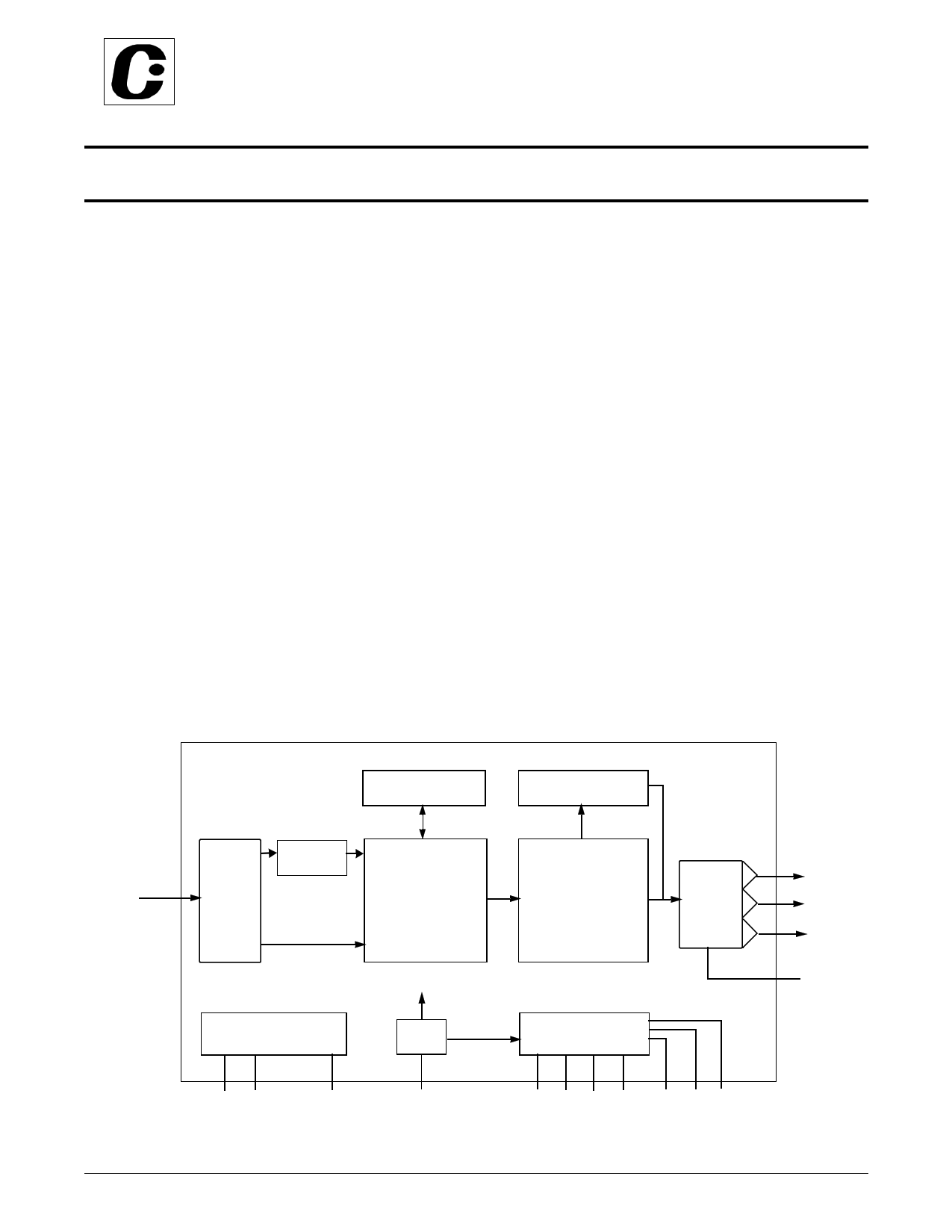
LINE
MEMORY
YUV-RGB CONVERTER
D[15:0]
PIXEL DATA
DIGITAL
INPUT
INTERFACE
RGB-YUV
CONVERTER
TRUE SCALE
SCALING &
DEFLICKERING
ENGINE
I2C REGISTER &
CONTROL BLOCK
SYSTEM CLOCK
PLL
NTSC/PAL
ENCODER
& FILTERS
TRIPLE
DAC
TIMING & SYNC
GENERATOR
Y/R
C/G
CVBS/B
RSET
SC SD
RESET*
XCLK
H V XI XO/FIN CSYNC P-OUT DS/BCO
Figure 1: Functional Block Diagram
201-0000-026 Rev 2.1, 8/2/99 *Intel I740 is a Trademark of Intel Corp.
1
1 page 
CHRONTEL
CH7006C
Table 1. Pin Descriptions
44-Pin
PLCC
44Pin
TQFP
Type
30 24
In
28 22 Out
27 21 Out
26 20 Out
23 17 Out
32 26 In/Out
33 27
In
35 29
In
40 34 Power
37 31 Power
31 25 Power
Symbol
Description
RSET
Y/R
C/G
CVBS/B
CSYNC
SD
SC
Reset*
AGND
AVDD
VDD
Reference Resistor
A 360 Ω resistor with short and wide traces should be attached
between RSET and ground. No other connections should be made to
this pin.
Luminance Output
A 75 Ω termination resistor with short traces should be attached
between Y and ground for optimum performance. In normal operating
modes other than SCART and RGB bypass, this pin outputs the
composite video signal. In SCART and RGB Bypass modes, this pin
outputs the red signal.
Chrominance Output
A 75 Ω termination resistor with short traces should be attached
between C and ground for optimum performance. In normal operating
modes other than SCART and RGB bypass, this pin outputs the
composite video signal. In SCART and RGB Bypass modes, this pin
outputs the green signal.
Composite Video Output
A 75 Ω termination resistor with short traces should be attached
between CVBS and ground for optimum performance. In normal
operating modes other than SCART and RGB bypass, this pin outputs
the composite video signal. In SCART and RGB Bypass modes, this pin
outputs the blue signal.
Composite Sync Output
A 75 Ω termination resistor with short traces should be attached
between CSYNC and ground for optimum performance. In SCART
mode, this pin outputs the composite sync signal.
Serial Data (External pull-up required)
This pin functions as the serial data pin of the I2C interface port (see the
I2C Port Operation section for details). This pin uses the DVDD supply
and is not 5V tolerant.
Serial Clock (Internal pull-up)
This pin functions as the serial clock pin of the I2C interface port (see
the I2C Port Operation section for details). This pin uses the DVDD
supply and is not 5V tolerant.
Reset Input
When this pin is low, the CH7006 is held in the power-on reset
condition. When this pin is high, the device operates normally and
reset is controlled through the I2C register.
Analog ground
This pin provides the ground reference for the analog section of the
CH7006, and MUST be connected to the system ground, to prevent
latchup. Refer to the Application Information section for information on
proper supply decoupling.
Analog Supply Voltage
This pins supplies the 5V power to the analog section of the CH7006.
DAC Power Supply
This pins supplies the 5V power to CH7006’s internal DAC’s.
201-0000-026 Rev 2.1, 8/2/99
5
5 Page 
CHRONTEL
CH7006C
When IDF = 9 (YCrCb 8-bit mode), H and V sync signals can be embedded into the data stream. In this mode, the
embedded sync will follow the CCIR656 convention, and the first byte of the “video timing reference code” will be
assumed to occur when a Cb sample would occur if the video stream was continuous. This is delineated in Table 8
shown below.
.
Table 8. YCrCb Multiplexed Mode with Embedded Syncs
IDF#
Format
9
YCrCb 8-bit
Pixel#
P0a P0b P1a P1b P2a P2b P3a P3b
Bus Data
D[7]
FF
00
00
S[7]
Cb2[7] Y2[7]
Cr2[7] Y3[7]
D[6] FF
00
00
S[6]
Cb2[6] Y2[6]
Cr2[6] Y3[6]
D[5] FF
00
00
S[5]
Cb2[5] Y2[5]
Cr2[5] Y3[5]
D[4] FF
00
00
S[4]
Cb2[4] Y2[4]
Cr2[4] Y3[4]
D[3] FF
00
00
S[3]
Cb2[3] Y2[3]
Cr2[3] Y3[3]
D[2] FF
00
00
S[2]
Cb2[2] Y2[2]
Cr2[2] Y3[2]
D[1] FF
00
00
S[1]
Cb2[1] Y2[1]
Cr2[1] Y3[1]
D[0] FF
00
00
S[0]
Cb2[0] Y2[0]
Cr2[0] Y3[0]
In this mode the S[7.0} contains the following data:
S[6] = F = 1 during field 2, 0 during field 1
S[5] = V = 1 during field blanking, 0 elsewhere
S[4] = H = 1 during EAV (the synchronization reference at the end of active video)
0 during SAV (the synchronization reference at the start of active video)
Bits S[7] and S[3-0] are ignored.
HSYNC
POut/
XCLK
tHD
Pixel
DD[7at:a0]
tHSW
tP3 tPH3
tSP3 tHP3
P0a P0b P0c P1a P1b P1c
Figure 6: Multiplexed Pixel Data Transfer Mode (IDF = 6)
Table 9. RGB 8-bit Multiplexed Mode (24-bit Color)
IDF#
Format
6
RGB 8-bit
Pixel#
Bus Data
D[7]
D[6]
D[5]
D[4]
D[3]
D[2]
D[1]
D[0]
P0a
B0[7]
B0[6]
B0[5]
B0[4]
B0[3]
B0[2]
B0[1]
B0[0]
P0b
G0[7]
G0[6]
G0[5]
G0[4]
G0[3]
G0[2]
G0[1]
G0[0]
P0c
R0[7]
R0[6]
R0[5]
R0[4]
R0[3]
R0[2]
R0[1]
R0[0]
P1a
B1[7]
B1[6]
B1[5]
B1[4]
B1[3]
B1[2]
B1[1]
B1[0]
P1b
G1[7]
G1[6]
G1[5]
G1[4]
G1[3]
G1[2]
G1[1]
G1[0]
P1c
R1[7]
R1[6]
R1[5]
R1[4]
R1[3]
R1[2]
R1[1]
R1[0]
P2a
B2[7]
B2[6]
B2[5]
B2[4]
B2[3]
B2[2]
B2[1]
B2[0]
P2b
G2[7]
G2[6]
G2[5]
G2[4]
G2[3]
G2[2]
G2[1]
G2[0]
P2c
R2(7)
R2(6)
R2(5)
R2(4)
R2(3)
R2(2)
R2(1)
R2(0)
201-0000-026 Rev 2.1, 8/2/99
11
11 Page | ||
| Páginas | Total 30 Páginas | |
| PDF Descargar | [ Datasheet CH7006C-T.PDF ] | |
Hoja de datos destacado
| Número de pieza | Descripción | Fabricantes |
| CH7006C-T | Digital PC to TV Encoder Features | ETC |
| CH7006C-V | Digital PC to TV Encoder Features | ETC |
| Número de pieza | Descripción | Fabricantes |
| SLA6805M | High Voltage 3 phase Motor Driver IC. |
Sanken |
| SDC1742 | 12- and 14-Bit Hybrid Synchro / Resolver-to-Digital Converters. |
Analog Devices |
|
DataSheet.es es una pagina web que funciona como un repositorio de manuales o hoja de datos de muchos de los productos más populares, |
| DataSheet.es | 2020 | Privacy Policy | Contacto | Buscar |