|
|
|
PDF CH7008A-T Data sheet ( Hoja de datos )
| Número de pieza | CH7008A-T | |
| Descripción | Digital PC to TV Encoder Features | |
| Fabricantes | ETC | |
| Logotipo | ||
Hay una vista previa y un enlace de descarga de CH7008A-T (archivo pdf) en la parte inferior de esta página. Total 30 Páginas | ||
|
No Preview Available !
CHRONTEL
CH7008A
Digital PC to TV Encoder Features
Features
• Support for low voltage interface to VGA controller
• Universal digital interface accepts YCrCb (CCIR656)
or RGB (15, 16 or 24-bit multiplexed) video data in
both non-interlaced and interlaced formats
• TrueScale TM rendering engine supports underscan
operations for various graphic resolutions† ¥
• Enhanced text sharpness and adaptive flicker removal
with up to 5-lines of filtering†
• Enhanced dot crawl control and area reduction
• Fully programmable through I2C port
• Supports NTSC, NTSC-EIA (Japan), and PAL (B, D,
G, H, I, M and N) TV formats
• Provides Composite, S-Video and SCART outputs
• Auto-detection of TV presence
• Programmable power management
• 9-bit video DAC outputs
• Complete Windows and DOS driver software
• Offered in 44-pin PLCC, 44-pin TQFP
General Description
Chrontel’s CH7008 digital PC to TV encoder is a stand-
alone integrated circuit which provides a PC 99 compliant
solution for TV output on non-DVD enabled systems.
Suggested application use with the Intel 810 chipset &
Intel 810E chipset.* It provides a universal digital input
port to accept a pixel data stream from a compatible VGA
controller (or equivalent) and converts this directly into
NTSC or PAL TV format.
This circuit integrates a digital NTSC/PAL encoder with
9-bit DAC interface, and new adaptive flicker filter, and
high accuracy low-jitter phase locked loop to create
outstanding quality video. Through its TrueScaleTM
scaling and deflickering engine, the CH7008 supports full
vertical and horizontal underscan capability and operates
in 5 different resolutions including 640x480 and 800x600.
A new universal digital interface along with full
programmability make the CH7008 ideal for system-level
PC solutions. All features are software programmable
through a standard I2C port, to enable a complete PC
solution using a TV as the primary display.
† Patent number 5,781,241
¥ Patent number 5,914,753
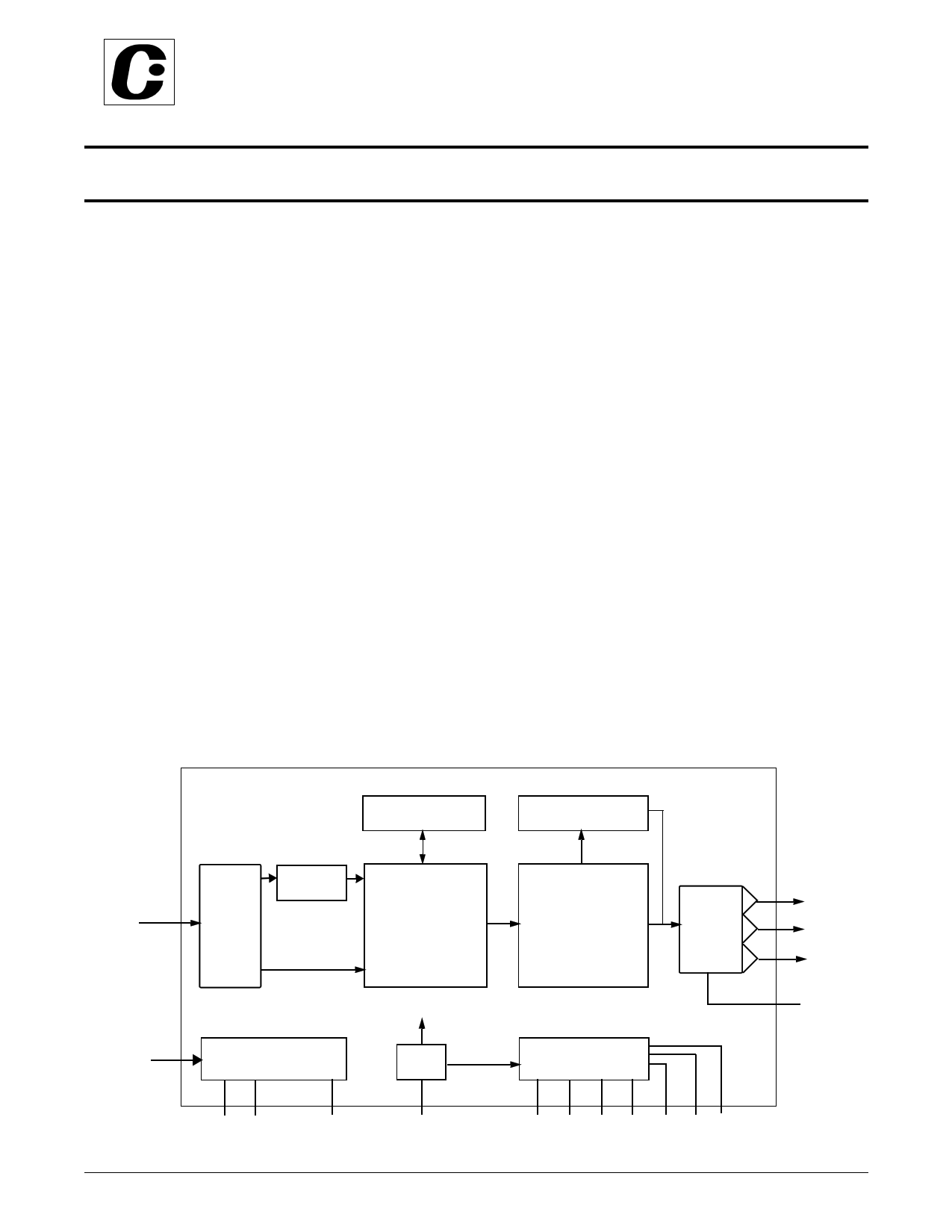
LINE
MEMORY
D[11:0]
PIXEL DATA
DIGITAL
INPUT
INTERFACE
RGB-YUV
CONVERTER
TRUE SCALE
SCALING &
DEFLICKERING
ENGINE
YUV-RGB CONVERTER
NTSC/PAL
ENCODER
& FILTERS
TRIPLE
DAC
GPIO[1:0]
I2C REGISTER &
CONTROL BLOCK
SYSTEM CLOCK
PLL
TIMING & SYNC
GENERATOR
SC SD
RESET*
XCLK*
H V XI/FIN XO CSYNC P-OUT DS/BCO
Figure 1: Functional Block Diagram
201-0000-027 Rev 2.2, 9/30/99 *Intel 810 and Intel 810E are Trademarks of Intel Corp
Y/R
C/G
CVBS/B
ISET
1
1 page 
CHRONTEL
CH7008A
Table 1. Pin Descriptions
44-Pin
PLCC
44-Pin
TQFP
Type
32 26 In/Out
33 27 In
35 29 In
38 32 In
39 33 Out
41 35 In/Out
43 37 Out
11,22,36
14,24,34,
42
25,29
31
37
40
44
5,16,30
8,18,28,3
6
19,23
25
31
34
38
Power
Power
Power
Power
Power
Power
Power
Symbol
Description
SD
SC
RESET*
XI/FIN
XO
DS/BCO
Serial Data Input/Output
This pin functions as the serial data pin of the I2C interface port, and
uses the DVDD supply.
(see the I2C Port Operation section for details)
Serial Clock Input
This pin functions as the serial clock pin of the I2C interface port, and
uses the DVDD supply.
(see the I2C Port Operation section for details)
Reset* Input
When this pin is low, the CH7008 is held in the power-on reset
condition. When this pin is high, the device operates normally and reset
is controlled through the I2C register.
Crystal Input/External Reference Input
A parallel resonance 14.31818MHz crystal should be attached
between this pin and XO. However, an external CMOS clock can be
attached to XI/FIN.
Crystal Output
A parallel resonance 14.31818MHz +20ppm crystal should be
attached between this pin and XI/FIN. However, if an external CMOS
clock is attached to XI/FIN, XO should not be connected.
Data start (input)/Buffered Clock (output)
In normal operating modes, when configured as an input, the rising
edge of this signal identifies the first active pixel of data for each
active line. The level is 0 to DVDD2, with VREF as the threshold level.
P-OUT
DVDD
DGND
When configured as an output this pin provides a buffered clock
output, driven by the DVDD supply. The output clock can be selected
using the BCO register (17th) (see Registers and Programing).
Pixel Clock Output
This pin provides a pixel clock signal to the VGA controller (adjustable as
1X, 2X and 3X) and is driven from the DVDD2 supply. This clock will only
be provided in master clock modes, and will be tri-stated otherwise, (see
the section on Digital Video Interface and Registers and Programming
for more details). The capacitive loading on this pin should be kept to a
minimum.
Digital Supply Voltage
Digital Ground
GND
VDD
AVDD
AGND
DVDD2
DAC
DAC Supply Voltage
PLL Supply Voltage
PLL Ground
I/O SUPPLY VOLTAGE
Digital supply voltage for the P-OUT
201-0000-027 Rev 2.2, 9/30/99
5
5 Page 
CHRONTEL
CH7008A
Display Modes (continued)
It is designed to support output to either NTSC or PAL television formats. The CH7008 provides interpolated
scaling with selectable factors of 5:4, 1:1, 7:8, 5:6, 3:4 and 7:10 in order to support adjustable overscan or underscan
operation when displayed on a TV. This combination of factors results in a matrix of useful operating modes which
are listed in detail in Table 7.
Table 7. CH7008 Display Modes
TV Format
Standard
NTSC
NTSC
NTSC
NTSC
NTSC
NTSC
NTSC
NTSC
NTSC
NTSC
NTSC
NTSC
NTSC
Input
(active)
Resolution
640x480
640x480
640x480
800x600
800x600
800x600
640x400
640x400
640x400
720x400
720x400
512x384
512x384
Scale
Factor
1:1
7:8
5:6
5:6
3:4
7:10
5:4
1:1
7:8
5:4
1:1
5:4
1:1
Active
TV Lines
Percent (1)
Overscan
480 10%
420 (3%)
400 (8%)
500 16%
450 4%
420 (3%)
500 16%
400 (8%)
350 (19%)
500 16%
400 (8%)
480 10%
384 (11%)
Pixel
Clock
24.671
28.196
30.210
39.273
43.636
47.832
21.147
26.434
30.210
23.790
29.455
20.140
24.671
Horizontal Vertical
Total
Total
784
784
800
1040
1040
1064
840
840
840
945
936
800
784
525
600
630
630
700
750
420
525
600
420
525
420
525
PAL
640x480
5:4
600
14%
21.000
840
500
PAL
640x480
1:1
480
(8%)
26.250
840
625
PAL
640x480
5:6
400
(29%)
31.500
840
750
PAL
800x600
1:1
600
14%
29.500
944
625
PAL
800x600
5:6
500
(4%)
36.000
960
750
PAL
800x600
3:4
450
(15%)
39.000
936
836
PAL
640x400
5:4
500
(4%)
25.000
1000
500
PAL
640x400
1:1
400
(29%)
31.500
1008
625
PAL
720x400
5:4
500
(4%)
28.125
1125
500
PAL
720x400
1:1
400
(29%)
34.875
1116
625
PAL
512x384
5:4
480
(8%)
21.000
840
500
PAL
512x384
1:1
384
(35%)
26.250
840
625
(1) Note: Percent underscan is a calculated value based on average viewable lines on each TV format, assuming an average TV over-
scan of 10%. (Negative values) indicate modes which are operating in underscan.
For NTSC: 480 active lines - 10% (overscan) = 432 viewable lines (average)
For PAL: 576 active lines - 10% (overscan) = 518 viewable lines (average)
The inclusion of multiple levels of scaling for each resolution have been created to enable optimal use of the
CH7008 for different application needs. In general, underscan (modes where percent overscan is negative) provides
an image that is viewable in its entirety on screen; it should be used as the default for most applications (e.g.,
viewing text screens, operating games, running productivity applications and working within Windows).
Overscanning provides an image that extends past the edges of the TV screen, exactly like normal television
programs and movies appear on TV, and is only recommended for viewing movies or video clips coming from the
computer. In addition to the above mode table, the CH7008 also support interlaced input modes, both in CCIR 656
and proprietary formats (see Display Mode Register section).
Flicker Filter and Text Enhancement
The CH7008 integrates an advanced 2-line, 3-line, 4-line and 5-line (depending on mode) vertical deflickering filter
circuit to help eliminate the flicker associated with interlaced displays. This flicker circuit provides an adaptive filter
algorithm for implementing flicker reduction with selections of high, medium or low flicker content for both luma
and chroma channels (see register descriptions). In addition, a special text enhancement circuit incorporates
201-0000-027 Rev 2.2, 9/30/99
11
11 Page | ||
| Páginas | Total 30 Páginas | |
| PDF Descargar | [ Datasheet CH7008A-T.PDF ] | |
Hoja de datos destacado
| Número de pieza | Descripción | Fabricantes |
| CH7008A-T | Digital PC to TV Encoder Features | ETC |
| CH7008A-V | Digital PC to TV Encoder Features | ETC |
| Número de pieza | Descripción | Fabricantes |
| SLA6805M | High Voltage 3 phase Motor Driver IC. |
Sanken |
| SDC1742 | 12- and 14-Bit Hybrid Synchro / Resolver-to-Digital Converters. |
Analog Devices |
|
DataSheet.es es una pagina web que funciona como un repositorio de manuales o hoja de datos de muchos de los productos más populares, |
| DataSheet.es | 2020 | Privacy Policy | Contacto | Buscar |