|
|
|
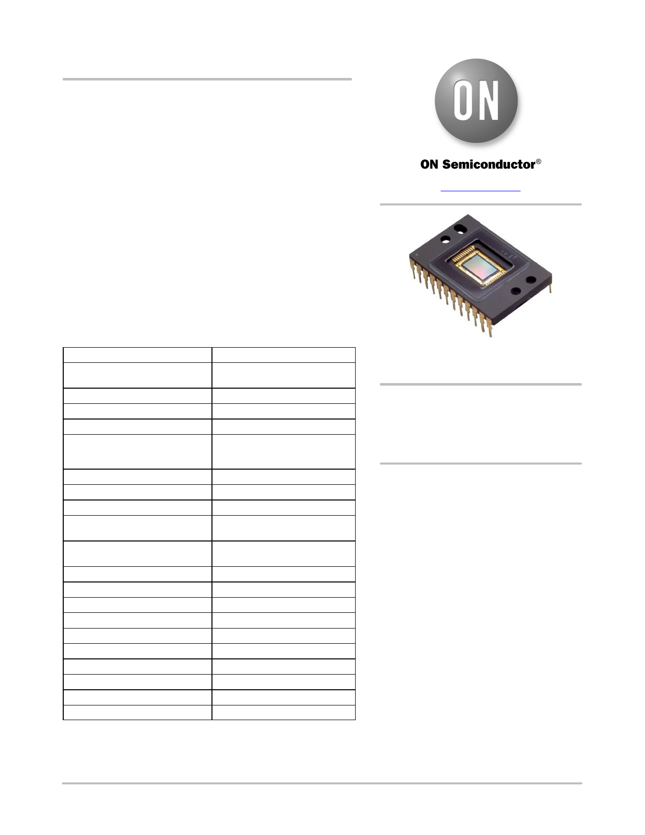
PDF KAF-0402-AAA Data sheet ( Hoja de datos )
| Número de pieza | KAF-0402-AAA | |
| Descripción | CCD Image Sensor | |
| Fabricantes | ON Semiconductor | |
| Logotipo | ||
Hay una vista previa y un enlace de descarga de KAF-0402-AAA (archivo pdf) en la parte inferior de esta página. Total 16 Páginas | ||
|
No Preview Available !
KAF-0402
768 (H) x 512 (V) Full Frame
CCD Image Sensor
Description
The KAF−0402 Image Sensor is a high performance area CCD
(charge-coupled device) image sensor with 768 (H) × 512 (V)
photoactive pixels designed for a wide range of image sensing
applications.
The sensor incorporates true two-phase CCD technology,
simplifying the support circuits required to drive the sensor as well as
reducing dark current without compromising charge capacity.
The sensor also utilizes the TRUESENSE Transparent Gate Electrode
to improve sensitivity compared to the use of a standard front side
illuminated polysilicon electrode.
Optional microlenses focus the majority of the light through the
transparent gate, increasing the optical response further.
Table 1. GENERAL SPECIFICATIONS
Parameter
Typical Value
Architecture
Full Frame CCD, Enhanced
Response
Total Number of Pixels
784 (H) × 520 (V)
Number of Active Pixels
768 (H) × 512 (V) = approx. 0.4 Mp
Pixel Size
9.0 mm (H) × 9.0 mm (V)
Active Image Size
6.91 mm (H) × 4.6 mm (V)
8.3 mm (Diagonal)
1/2″ Optical Format
Die Size
8.4 mm (H) × 5.5 mm (V)
Aspect Ratio
3:2
Saturation Signal
100,000 electrons
Quantum Efficiency
(with Microlens)
Peak: 77%
400 nm: 45%
Quantum Efficiency
(No Microlens)
Peak: 65%
400 nm: 30%
Output Sensitivity
10 mV/e−
Read Noise
Dark Current
15 electrons
< 10 pA/cm2 at 25°C
Dark Current Doubling Temperature 6.3°C
Dynamic Range
76 dB
Charge Transfer Efficiency
> 0.99999
Blooming Suppression
None
Maximum Date Rate
10 MHz
Package
CERDIP Package (Sidebrazed)
Cover Glass
Clear or AR Coated, 2 Sides
NOTE: Parameters above are specified at T = 25°C unless otherwise noted.
www.onsemi.com
Figure 1. KAF−0402 Full Frame CCD
Image Sensor
Applications
• Digitization
• Medical
• Scientific
ORDERING INFORMATION
See detailed ordering and shipping information on page 2 of
this data sheet.
© Semiconductor Components Industries, LLC, 2015
April, 2015 − Rev. 2
1
Publication Order Number:
KAF−0402/D
1 page 
Physical Description
Pin Description and Device Orientation
KAF−0402
VOG 1
VOUT 2
VDD 3
VRD 4
fR 5
VSS 6
fH1 7
fH2 8
N/C 9
N/C 10
VSUB 11
N/C 12
Pin 1
Pixel 1,1
24 N/C
23 GUARD
22 fV1
21 fV1
20 fV2
19 fV2
18 fV2
17 fV2
16 fV1
15 fV1
14 VSUB
13 N/C
Figure 5. Pinout Diagram
Table 4. PIN DESCRIPTION
Pin Name
Description
1
VOG
Output Gate
2
VOUT
Video Output
3
VDD
Amplifier Supply
4
VRD
Reset Drain
5 fR Reset Clock
6
VSS
Amplifier Supply Return
7 fH1 Horizontal CCD Clock − Phase 1
8 fH2 Horizontal CCD Clock − Phase 2
9 N/C No Connection
10 N/C No Connection
11 VSUB Substrate
12 N/C No Connection
Pin Name
Description
13 N/C No Connection
14 VSUB Substrate
15 fV1 Vertical CCD Clock − Phase 1
16 fV1 Vertical CCD Clock − Phase 1
17 fV2 Vertical CCD Clock − Phase 2
18 fV2 Vertical CCD Clock − Phase 2
19 fV2 Vertical CCD Clock − Phase 2
20 fV2 Vertical CCD Clock − Phase 2
21 fV1 Vertical CCD Clock − Phase 1
22 fV1 Vertical CCD Clock − Phase 1
23 GUARD Guard Ring
24 N/C No Connection
www.onsemi.com
5
5 Page 
KAF−0402
TIMING
Table 10. REQUIREMENTS AND CHARACTERISTICS
Description
Symbol
Minimum
Nominal
Maximum
Units
Notes
fH1, fH2 Clock Frequency
fH
−
4
10
MHz
1, 2, 3
Pixel Period (1 Count)
tPIX 100 250
−
ns
fH1, fH2 Set-up Time
tfHS
0.5
1
− ms
fV1, fV2 Clock Pulse Width
tfV 1.5
2
− ms 2
Reset Clock Pulse Width
tfR 10 20 − ns 4
Readout Time
tREADOUT
43.7
107
−
ms
5
Integration Time
tINT − − −
6
Line Time
tLINE
84.1
206
−
ms
7
1. 50% duty cycle values.
2. CTE may degrade above the nominal frequency.
3. Rise and fall times (10/90% levels) should be limited to 5−10% of clock period. Crossover of register clocks should be between 40−60% of
amplitude.
4. fR should be clocked continuously.
5. tREADOUT = (520 ⋅ tLINE)
6. Integration time (tINT) is user specified. Longer integration times will degrade noise performance due to dark signal fixed pattern and shot
noise.
7. tLINE = (3 ⋅ tfV) + tfHS + (796 ⋅ tPIX) + tPIX
Frame Timing
fV1
fV2
fH1
fH2
tINT
Line
Frame Timing
tREADOUT
1 Frame = 520 Lines
12
519
520
Figure 9. Frame Timing Diagram
www.onsemi.com
11
11 Page | ||
| Páginas | Total 16 Páginas | |
| PDF Descargar | [ Datasheet KAF-0402-AAA.PDF ] | |
Hoja de datos destacado
| Número de pieza | Descripción | Fabricantes |
| KAF-0402-AAA | CCD Image Sensor | ON Semiconductor |
| Número de pieza | Descripción | Fabricantes |
| SLA6805M | High Voltage 3 phase Motor Driver IC. |
Sanken |
| SDC1742 | 12- and 14-Bit Hybrid Synchro / Resolver-to-Digital Converters. |
Analog Devices |
|
DataSheet.es es una pagina web que funciona como un repositorio de manuales o hoja de datos de muchos de los productos más populares, |
| DataSheet.es | 2020 | Privacy Policy | Contacto | Buscar |