|
|
PDF MTB3N100E Data sheet ( Hoja de datos )
| Número de pieza | MTB3N100E | |
| Descripción | High Energy Power FET | |
| Fabricantes | ON Semiconductor | |
| Logotipo | ||
Hay una vista previa y un enlace de descarga de MTB3N100E (archivo pdf) en la parte inferior de esta página. Total 11 Páginas | ||
|
No Preview Available !
MTB3N100E
Designer’s™ Data Sheet
TMOS E−FET.™
High Energy Power FET
D2PAK for Surface Mount
N−Channel Enhancement−Mode Silicon
Gate
http://onsemi.com
TMOS POWER FET
The D2PAK package has the capability of housing a larger die than
any existing surface mount package which allows it to be used in
applications that require the use of surface mount components with
higher power and lower RDS(on) capabilities. This high voltage
MOSFET uses an advanced termination scheme to provide enhanced
voltage−blocking capability without degrading performance over
time. In addition, this advanced TMOS E−FET is designed to
withstand high energy in the avalanche and commutation modes. The
new energy efficient design also offers a drain−to−source diode with a
fast recovery time. Designed for high voltage, high speed switching
applications in power supplies, converters and PWM motor controls,
these devices are particularly well suited for bridge circuits where
diode speed and commutating safe operating areas are critical and
offer additional safety margin against unexpected voltage transients.
3.0 AMPERES, 1000 VOLTS
RDS(on) = 4.0 W
CASE 418B−02, Style 2
D2PAK
D
• Robust High Voltage Termination
• Avalanche Energy Specified
®G
• Source−to−Drain Diode Recovery Time Comparable to a
Discrete Fast Recovery Diode
• Diode is Characterized for Use in Bridge Circuits
• IDSS and VDS(on) Specified at Elevated Temperature
• Short Heatsink Tab Manufactured — Not Sheared
• Specially Designed Leadframe for Maximum Power Dissipation
• Available in 24 mm 13−inch/800 Unit Tape & Reel, Add T4 Suffix to Part Number
S
© Semiconductor Components Industries, LLC, 2006
August, 2006 − Rev. 3
1
Publication Order Number:
MTB3N100E/D
1 page 
MTB3N100E
POWER MOSFET SWITCHING
Switching behavior is most easily modeled and predicted
by recognizing that the power MOSFET is charge
controlled. The lengths of various switching intervals (Δt)
are determined by how fast the FET input capacitance can
be charged by current from the generator.
The published capacitance data is difficult to use for
calculating rise and fall because drain−gate capacitance
varies greatly with applied voltage. Accordingly, gate
charge data is used. In most cases, a satisfactory estimate
of average input current (IG(AV)) can be made from a
rudimentary analysis of the drive circuit so that
t = Q/IG(AV)
During the rise and fall time interval when switching a
resistive load, VGS remains virtually constant at a level
known as the plateau voltage, VSGP. Therefore, rise and fall
times may be approximated by the following:
tr = Q2 x RG/(VGG − VGSP)
tf = Q2 x RG/VGSP
where
VGG = the gate drive voltage, which varies from zero to VGG
RG = the gate drive resistance
and Q2 and VGSP are read from the gate charge curve.
During the turn−on and turn−off delay times, gate current is
not constant. The simplest calculation uses appropriate
values from the capacitance curves in a standard equation
for voltage change in an RC network. The equations are:
td(on) = RG Ciss In [VGG/(VGG − VGSP)]
td(off) = RG Ciss In (VGG/VGSP)
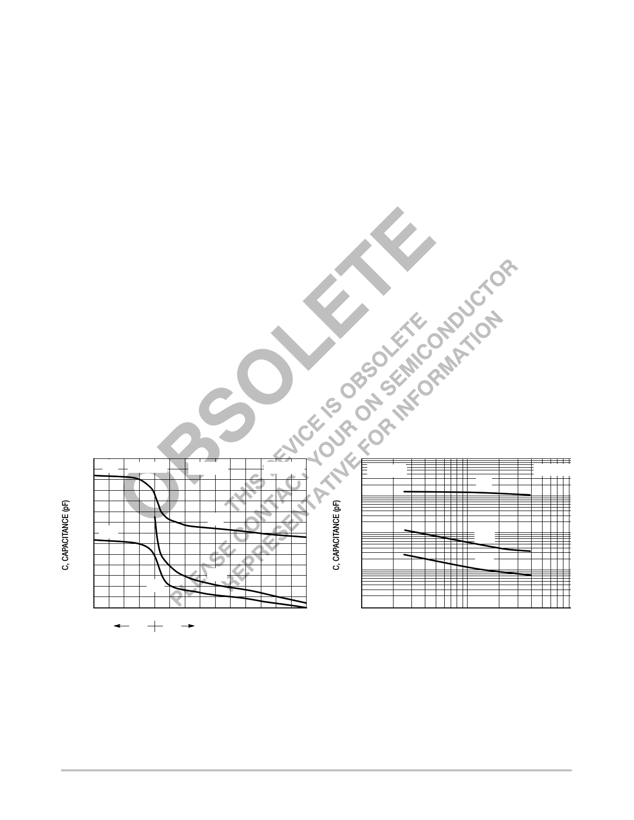
The capacitance (Ciss) is read from the capacitance curve
at a voltage corresponding to the off−state condition when
calculating td(on) and is read at a voltage corresponding to
the on−state when calculating td(off).
At high switching speeds, parasitic circuit elements
complicate the analysis. The inductance of the MOSFET
source lead, inside the package and in the circuit wiring
which is common to both the drain and gate current paths,
produces a voltage at the source which reduces the gate
drive current. The voltage is determined by Ldi/dt, but since
di/dt is a function of drain current, the mathematical solution
is complex. The MOSFET output capacitance also
complicates the mathematics. And finally, MOSFETs have
finite internal gate resistance which effectively adds to the
resistance of the driving source, but the internal resistance
is difficult to measure and, consequently, is not specified.
The resistive switching time variation versus gate
resistance (Figure 9) shows how typical switching
performance is affected by the parasitic circuit elements. If
the parasitics were not present, the slope of the curves
would maintain a value of unity regardless of the switching
speed. The circuit used to obtain the data is constructed to
minimize common inductance in the drain and gate circuit
loops and is believed readily achievable with board
mounted components. Most power electronic loads are
inductive; the data in the figure is taken with a resistive load,
which approximates an optimally snubbed inductive load.
Power MOSFETs may be safely operated into an inductive
load; however, snubbing reduces switching losses.
2800
Ciss
2400
VDS = 0 V
VGS = 0 V
TJ = 25°C
2000
1600
Crss
1200
Ciss
800
Coss
400 Crss
0
10 5 0
5 10 15 20 25
VGS VDS
GATE−TO−SOURCE OR DRAIN−TO−SOURCE VOLTAGE (VOLTS)
Figure 7a. Capacitance Variation
10000
VGS = 0 V
1000
TJ = 25°C
Ciss
100
Coss
10 Crss
1
10 100 10
VDS, DRAIN−TO−SOURCE VOLTAGE (VOLTS)
Figure 7b. High Voltage Capacitance
Variation
http://onsemi.com
5
5 Page 
MTB3N100E
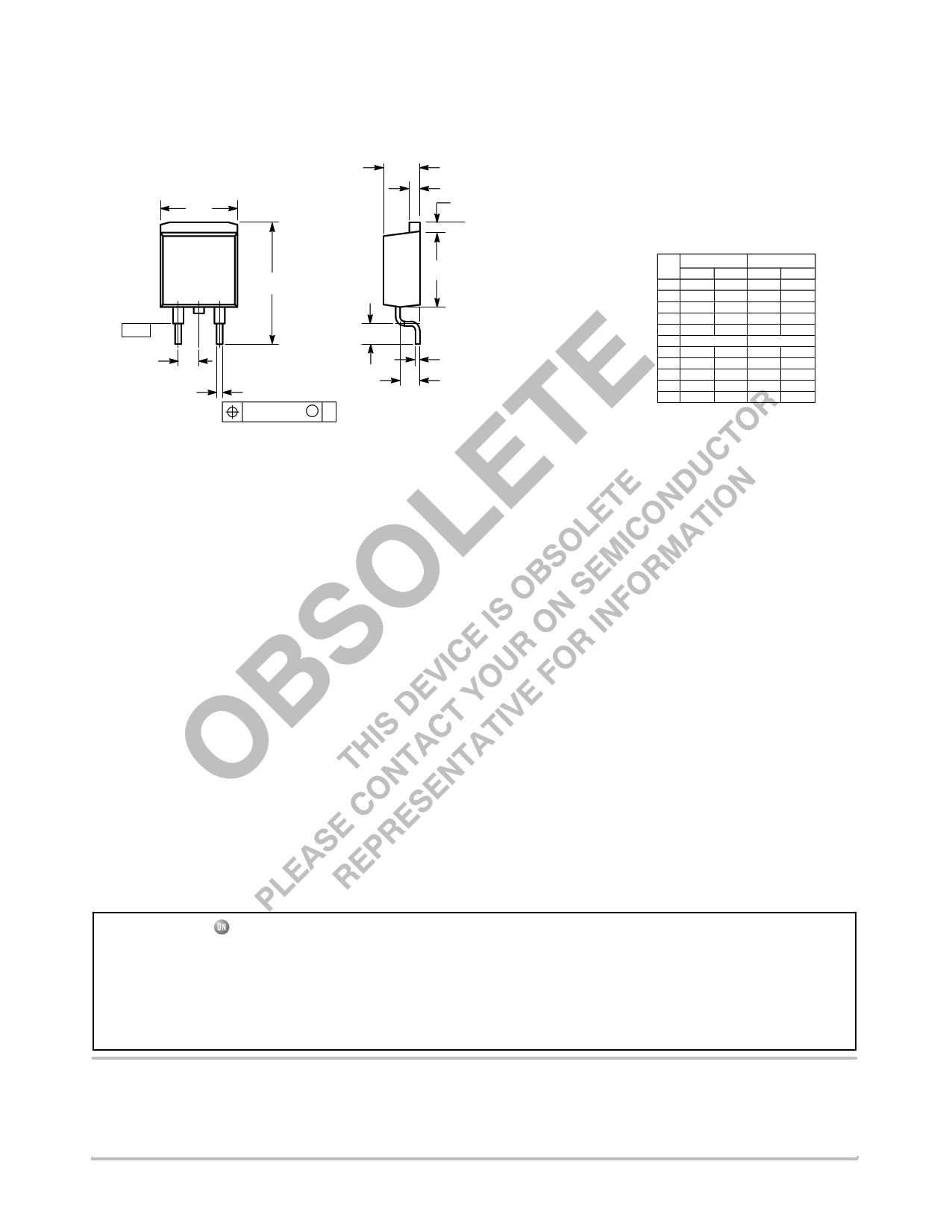
PACKAGE DIMENSIONS
CASE 418B−02
ISSUE B
C
E
BV
4
123
S
A
−T−
SEATING
PLANE
G
K
J
D 3 PL
0.13 (0.005) M T
H
STYLE 2:
PIN 1. GATE
2. DRAIN
3. SOURCE
4. DRAIN
NOTES:
1. DIMENSIONING AND TOLERANCING PER ANSI
Y14.5M, 1982.
2. CONTROLLING DIMENSION: INCH.
INCHES
DIM MIN MAX
A 0.340 0.380
B 0.380 0.405
C 0.160 0.190
D 0.020 0.035
E 0.045 0.055
G 0.100 BSC
H 0.080 0.110
J 0.018 0.025
K 0.090 0.110
S 0.575 0.625
V 0.045 0.055
MILLIMETERS
MIN MAX
8.64 9.65
9.65 10.29
4.06 4.83
0.51 0.89
1.14 1.40
2.54 BSC
2.03 2.79
0.46 0.64
2.29 2.79
14.60 15.88
1.14 1.40
ON Semiconductor and
are registered trademarks of Semiconductor Components Industries, LLC (SCILLC). SCILLC reserves the right to make changes without further notice
to any products herein. SCILLC makes no warranty, representation or guarantee regarding the suitability of its products for any particular purpose, nor does SCILLC assume any liability
arising out of the application or use of any product or circuit, and specifically disclaims any and all liability, including without limitation special, consequential or incidental damages.
“Typical” parameters which may be provided in SCILLC data sheets and/or specifications can and do vary in different applications and actual performance may vary over time. All
operating parameters, including “Typicals” must be validated for each customer application by customer’s technical experts. SCILLC does not convey any license under its patent rights
nor the rights of others. SCILLC products are not designed, intended, or authorized for use as components in systems intended for surgical implant into the body, or other applications
intended to support or sustain life, or for any other application in which the failure of the SCILLC product could create a situation where personal injury or death may occur. Should
Buyer purchase or use SCILLC products for any such unintended or unauthorized application, Buyer shall indemnify and hold SCILLC and its officers, employees, subsidiaries, affiliates,
and distributors harmless against all claims, costs, damages, and expenses, and reasonable attorney fees arising out of, directly or indirectly, any claim of personal injury or death
associated with such unintended or unauthorized use, even if such claim alleges that SCILLC was negligent regarding the design or manufacture of the part. SCILLC is an Equal
Opportunity/Affirmative Action Employer. This literature is subject to all applicable copyright laws and is not for resale in any manner.
PUBLICATION ORDERING INFORMATION
LITERATURE FULFILLMENT:
Literature Distribution Center for ON Semiconductor
P.O. Box 5163, Denver, Colorado 80217 USA
Phone: 303−675−2175 or 800−344−3860 Toll Free USA/Canada
Fax: 303−675−2176 or 800−344−3867 Toll Free USA/Canada
Email: [email protected]
N. American Technical Support: 800−282−9855 Toll Free
USA/Canada
Europe, Middle East and Africa Technical Support:
Phone: 421 33 790 2910
Japan Customer Focus Center
Phone: 81−3−5773−3850
http://onsemi.com
11
ON Semiconductor Website: www.onsemi.com
Order Literature: http://www.onsemi.com/orderlit
For additional information, please contact your local
Sales Representative
MTB3N100E/D
11 Page | ||
| Páginas | Total 11 Páginas | |
| PDF Descargar | [ Datasheet MTB3N100E.PDF ] | |
Hoja de datos destacado
| Número de pieza | Descripción | Fabricantes |
| MTB3N100E | TMOS POWER FET 3.0 AMPERES 1000 VOLTS | Motorola Semiconductors |
| MTB3N100E | High Energy Power FET | ON Semiconductor |
| Número de pieza | Descripción | Fabricantes |
| SLA6805M | High Voltage 3 phase Motor Driver IC. |
Sanken |
| SDC1742 | 12- and 14-Bit Hybrid Synchro / Resolver-to-Digital Converters. |
Analog Devices |
|
DataSheet.es es una pagina web que funciona como un repositorio de manuales o hoja de datos de muchos de los productos más populares, |
| DataSheet.es | 2020 | Privacy Policy | Contacto | Buscar |
