|
|
PDF DGD21084 Data sheet ( Hoja de datos )
| Número de pieza | DGD21084 | |
| Descripción | HALF BRIDGE GATE DRIVER | |
| Fabricantes | Diodes | |
| Logotipo |  |
|
Hay una vista previa y un enlace de descarga de DGD21084 (archivo pdf) en la parte inferior de esta página. Total 12 Páginas | ||
|
No Preview Available !
Description
The DGD21084 is a high voltage / high speed gate driver capable of
driving N-Channel MOSFETs and IGBTs in a half bridge configuration.
High voltage processing techniques enable the DGD21084’s high-side
to switch to 600V in a bootstrap operation.
The DGD21084 logic inputs are compatible with standard TTL and
CMOS levels (down to 3.3V) for easy interfacing with controlling
devices. The driver outputs feature high pulse current buffers
designed for minimum driver cross conduction. Programmable dead
time, by an external resistor, provides more system level flexibility.
The DGD21084 is offered in SO-14 (Type TH) package, the operating
temperature extends from -40°C to +125°C.
Applications
DC-DC Converters
DC-AC Inverters
AC-DC Power Supplies
Motor Controls
Class D Power Amplifiers
DGD21084
HALF BRIDGE GATE DRIVER IN SO-14
Features
Floating High-side Driver in Bootstrap Operation to 600V
Drives Two N-Channel MOSFETs or IGBTs in a Half Bridge
Configuation
Outputs Tolerant to Negative Transients
Programmable Dead Time to Protect MOSFETs
Wide Logic and Low-side Gate Driver Supply Voltage: 10V to
20V
Wide Logic Supply Voltage Offset Voltage: -5V to 5V
Logic Inputs (HIN and LIN*) 3.3V Capability
Schmitt Triggered Logic Inputs with Internal Pull Down
Undervoltage Lockout For High and Low Side Drivers
Extended Temperature Range: -40°C to +125°C
Totally Lead-Free & Fully RoHS Compliant (Notes 1 & 2)
Halogen and Antimony Free. “Green” Device (Note 3)
Mechanical Data
Case: SO-14 (Type TH)
Case Material: Molded Plastic. “Green” Molding Compound.
UL Flammability Classification Rating 94V-0
Moisture Sensitivity: Level 3 per J-STD-020
Terminals: Finish – Matte Tin Plated Leads, Solderable per
MIL-STD-202, Method 208
Weight: 0.142 grams (Approximate)
Typical Configuration
SO-14 (Type TH)
Top View
Ordering Information (Note 4)
Product
DGD21084S14-13
Marking
DGD21084
Reel Size (inches)
13
Tape Width (mm)
16
Quantity per Reel
2,500
Notes:
1. No purposely added lead. Fully EU Directive 2002/95/EC (RoHS) & 2011/65/EU (RoHS 2) compliant.
2. See http://www.diodes.com/quality/lead_free.html for more information about Diodes Incorporated’s definitions of Halogen- and Antimony-free, "Green"
and Lead-free.
3. Halogen- and Antimony-free "Green” products are defined as those which contain <900ppm bromine, <900ppm chlorine (<1500ppm total Br + Cl) and
<1000ppm antimony compounds.
4. For packaging details, go to our website at http://www.diodes.com/products/packages.html.
Marking Information
DGD21084
YY WW
= Manufacturer’s marking
DGD21084 = Product Type Marking Code
YY = Year (ex: 16 = 2016)
WW = Week (01 to 53)
DGD21084
Document Number DS38342 Rev. 1 - 2
1 of 12
www.diodes.com
April 2016
© Diodes Incorporated
1 page 
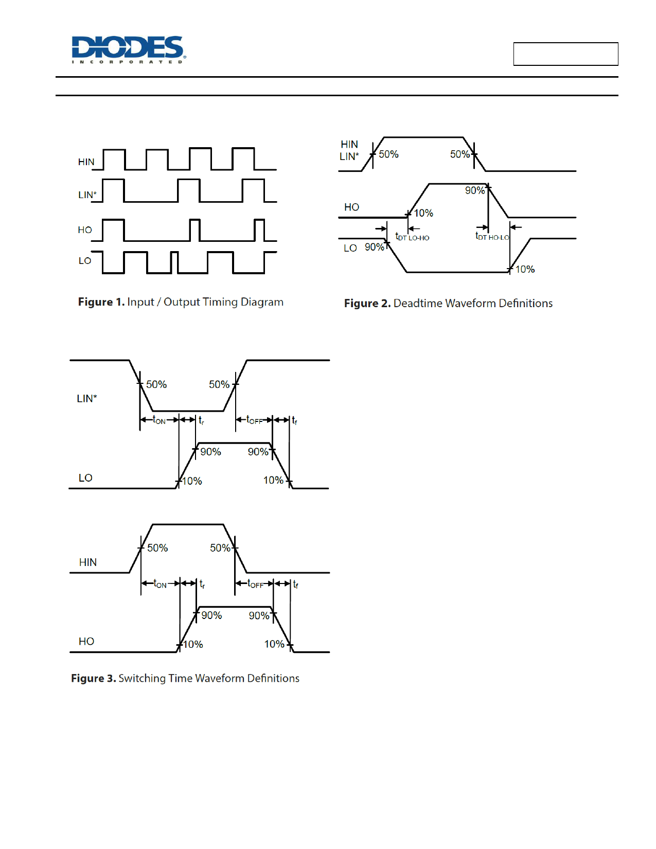
Timing Waveforms
DGD21084
DGD21084
Document Number DS38342 Rev. 1 - 2
5 of 12
www.diodes.com
April 2016
© Diodes Incorporated
5 Page 
Package Outline Dimensions
Please see http://www.diodes.com/package-outlines.html for the latest version.
SO-14 (Type TH)
D
E E1
A
e
b
h
Ø
A1
L
0.25
c
Gauge Plane
Seating Plane
DGD21084
SO-14 (Type TH)
Dim Min Max Typ
A 1.55 1.73 --
A1 0.10 0.25 --
b 0.35 0.51 --
c 0.190 0.248 --
D 8.56 8.74 8.61
E 5.84 6.20 6.00
E1 3.81 3.99 3.94
e -- -- 1.27
h -- -- 0.33
L 0.41 0.89 --
Ø 0 8 --
All Dimensions in mm
Suggested Pad Layout
Please see http://www.diodes.com/package-outlines.html for the latest version.
SO-14 (Type TH)
X
Y
Dimensions Value (in mm)
C 1.27
C1 C1 5.20
X 0.60
Y 2.20
C
Note:
For high voltage applications, the appropriate industry sector guidelines should be considered with regards to creepage and clearance distances between
device Terminals and PCB tracking.
DGD21084
Document Number DS38342 Rev. 1 - 2
11 of 12
www.diodes.com
April 2016
© Diodes Incorporated
11 Page | ||
| Páginas | Total 12 Páginas | |
| PDF Descargar | [ Datasheet DGD21084.PDF ] | |
Hoja de datos destacado
| Número de pieza | Descripción | Fabricantes |
| DGD2108 | HALF-BRIDGE GATE DRIVER | Diodes |
| DGD21084 | HALF BRIDGE GATE DRIVER | Diodes |
| Número de pieza | Descripción | Fabricantes |
| SLA6805M | High Voltage 3 phase Motor Driver IC. |
Sanken |
| SDC1742 | 12- and 14-Bit Hybrid Synchro / Resolver-to-Digital Converters. |
Analog Devices |
|
DataSheet.es es una pagina web que funciona como un repositorio de manuales o hoja de datos de muchos de los productos más populares, |
| DataSheet.es | 2020 | Privacy Policy | Contacto | Buscar |
