|
|
|
PDF NCP5425 Data sheet ( Hoja de datos )
| Número de pieza | NCP5425 | |
| Descripción | Dual Synchronous Buck Controller | |
| Fabricantes | ON Semiconductor | |
| Logotipo | ||
Hay una vista previa y un enlace de descarga de NCP5425 (archivo pdf) en la parte inferior de esta página. Total 22 Páginas | ||
|
No Preview Available !
NCP5425
Dual Synchronous
Buck Controller
The NCP5425 is a highly flexible dual buck controller with internal
gate drivers that can be used with two input power supplies and one or
two outputs in multiple configurations. The part contains all the
circuitry required for two independent synchronous dual NFET buck
regulators utilizing a feed forward voltage mode control method. The
NCP5425 can run from a single supply ranging from 4.6 to 12 V and
support a single two phase or dual single phase outputs. When used as
a dual output controller, the second output tracks voltage transients
from the first. Power blanking for low noise applications is supported
as well as independent cycle−by−cycle current limiting. The part is
available in a 20 pin TSSOP package allowing the designer to
minimize PCB area.
Features
• Operation Over 4.6 to 13.2 V
• Dual Synchronous Buck Design
• Configurable as a Single Two Phase Output or Two Single Phase
Outputs
• Programmable Power Sharing and Budgeting from Two Independent
Supplies
• 0.8 V "1% Reference for Low Voltage Outputs
• 1.5 A Peak Power Drive
• Switch Blanking for Noise Sensitive Applications through use of
ROSC Pin
• Programmable Frequency, 150 kHz to 750 kHz Operation
• Programmable Soft−Start
• Cycle−by−Cycle Overcurrent Protection
• Independent Programmable Current Limits
• 100% Duty Cycle for Fast Transient Response
• Internal Slope Compensation
• Out−of−Phase Synchronization between the Controllers
• Input Undervoltage Lockout
• On/Off Enable through use of the COMP Pins
• Power Supply Sequencing
• These are Pb−Free Devices
Applications
• DDR Memory Power
• Graphics Cards
http://onsemi.com
20
1
TSSOP−20
DB SUFFIX
CASE 948E
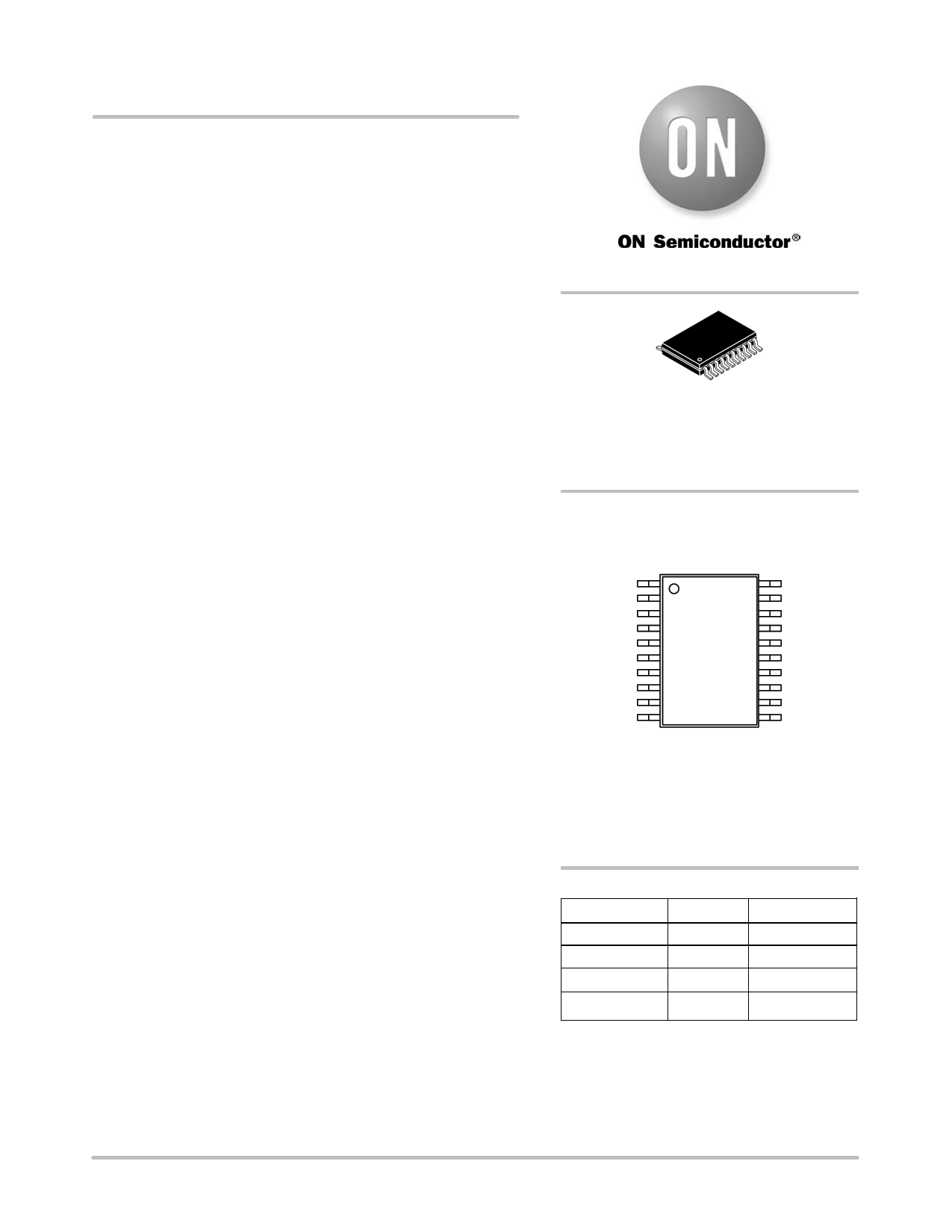
PIN CONNECTIONS AND
MARKING DIAGRAM
GATEH1
GATEL1
GND
BST
NC
NC
IS+1
IS−1
VFB1
COMP1
1
NCP
5425
ALYW G
G
20
GATEH2
GATEL2
VCC
ROSC
MODE
IS−2
IS+2
VREF2
VFB2
COMP2
A = Assembly Location
L = Wafer Lot
Y = Year
W = Work Week
G = Pb−Free Package
(Note: Microdot may be in either location)
ORDERING INFORMATION
Device
Package
Shipping†
NCP5425DB
TSSOP−20* 75 Units/Tube
NCP5425DBG TSSOP−20* 75 Units/Tube
NCP5425DBR2 TSSOP−20* 2500/Tape & Reel
NCP5425DBR2G TSSOP−20* 2500/Tape & Reel
†For information on tape and reel specifications,
including part orientation and tape sizes, please
refer to our Tape and Reel Packaging Specification
Brochure, BRD8011/D.
*This package is inherently Pb−Free.
© Semiconductor Components Industries, LLC, 2006
July, 2006 − Rev. 9
1
Publication Order Number:
NCP5425/D
1 page 
NCP5425
ELECTRICAL CHARACTERISTICS (continued) (0°C < TJ < 125°C; ROSC = 30.9 k, CCOMP1,2 = 0.1 mF, 4.75 V < VCC
< 13.2 V; 10.8 V < BST < 20 V, CGATE(H)1,2 = CGATE(L)1,2 = 1.0 nF; unless otherwise specified.)
Characteristic
Test Condition
Min Typ Max
OSCILLATOR
Switching Frequency
Switching Frequency
Switching Frequency
ROSC Voltage
Phase Difference
ROSC = 61.9 k; Measure GATE(H)1
ROSC = 30.9 k; Measure GATE(H)1
ROSC = 11.8 k; Measure GATE(H)1
ROSC = 30.9 k
−
112
224
562
0.970
−
150
300
750
1.000
180
188
376
938
1.030
−
Low Noise Disable
Guaranteed By Design
− 3.1 3.5
OVERCURRENT PROTECTION
OVC Comparator Offset Voltage
0 V < IS+1(2) < 5.5 V
0 V < IS−1(2) < 5.5 V
55 70 85
IS+1(2) Bias Current
IS−1(2) Bias Current
0 V < IS+1(2) < 5.5 V
0 V < IS−1(2) < 5.5 V
−1.0 0.1
−1.0 0.1
1.0
1.0
OVC Common Mode Range
− 0 − 5.5
SUPPLY CURRENTS
VCC Current
BST Current
COMP = 0 V (No Switching)
COMP = 0 V (No Switching)
− 16 22
− 3.5 6.0
UNDERVOLTAGE LOCKOUT
Start Threshold
GATE(H) Switching; COMP1(2) Charging
3.8 4.2 4.6
Stop Threshold
GATE(H) Not Switching; COMP1(2) Discharging
3.6
4.0
4.4
Hysteresis
Start−Stop
0.1 0.2 0.45
Unit
kHz
kHz
kHz
V
°
V
mV
mA
mA
V
mA
mA
V
V
V
http://onsemi.com
5
5 Page 
NCP5425
Inductor Current Sensing
Examples of lossless current sensing across an output
inductor are shown in Figure 8. Lx is the output inductance
and Rx represents its equivalent series resistance. To
compensate the current sense signal, the values of R1 and C1
are chosen so that Lx/Rx = R1 x C1. With these values, the
Switch
Node
current sense signal will have the same wave shape as the
inductor current and the voltage signal on C1 will represent
the instantaneous value of inductor current. The voltage
across C1 can be used as though it were a sense resistor with
the same value as the inductor’s ESR, thus avoiding a sense
resistor’s power loss.
Switch
Node
Lx R1
Rx
DC
Output
+ls
+
C1 Rx X IL
−
_
−ls
+
(8A)
70 mV
Lx R1
Rx
DC
Output
+ls
+
C1
R2
Rx*IL*R2
(R1 + R2)
− −ls _ +
(8B)
70 mV
Switch
Node
Switch
Node
Lx R1
Rx
DC
Output
+ls
+
C1 Rx X IL
−
_
−ls
+
R3
70 mV
(8C)
Lx R1
Rx
DC
Output
+ls
+
C1 (Rx*IL) + (ER3)
R3
(8D)
−
_
−ls
+
R4 70 mV
ER3 = (Vo*R3)/R3 + R4)
Figure 8. Inductor Current Sensing − Circuit Configurations
http://onsemi.com
11
11 Page | ||
| Páginas | Total 22 Páginas | |
| PDF Descargar | [ Datasheet NCP5425.PDF ] | |
Hoja de datos destacado
| Número de pieza | Descripción | Fabricantes |
| NCP5422A | (NCP5422A / NCP5423) Dual Out-of-Phase Synchronous Buck Controller | ON Semiconductor |
| NCP5423 | (NCP5422A / NCP5423) Dual Out-of-Phase Synchronous Buck Controller | ON Semiconductor |
| NCP5424 | Dual Synchronous Buck Controller | ON Semiconductor |
| NCP5424A | Dual Synchronous Buck Controller | ON Semiconductor |
| Número de pieza | Descripción | Fabricantes |
| SLA6805M | High Voltage 3 phase Motor Driver IC. |
Sanken |
| SDC1742 | 12- and 14-Bit Hybrid Synchro / Resolver-to-Digital Converters. |
Analog Devices |
|
DataSheet.es es una pagina web que funciona como un repositorio de manuales o hoja de datos de muchos de los productos más populares, |
| DataSheet.es | 2020 | Privacy Policy | Contacto | Buscar |