|
|
|
PDF MJE5852 Data sheet ( Hoja de datos )
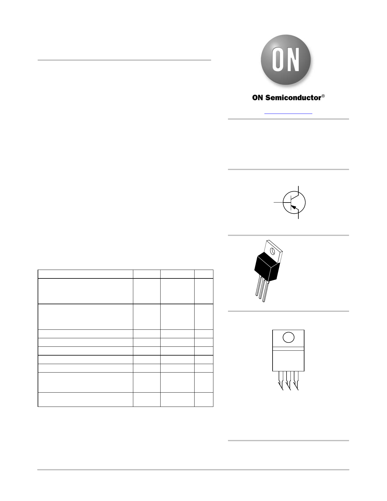
| Número de pieza | MJE5852 | |
| Descripción | Switch-mode Series PNP Silicon Power Transistors | |
| Fabricantes | ON Semiconductor | |
| Logotipo | ||
Hay una vista previa y un enlace de descarga de MJE5852 (archivo pdf) en la parte inferior de esta página. Total 8 Páginas | ||
|
No Preview Available !
MJE5850, MJE5851,
MJE5852
Switch-mode Series PNP
Silicon Power Transistors
The MJE5850, MJE5851 and the MJE5852 transistors are designed
for high−voltage, high−speed, power switching in inductive circuits
where fall time is critical. They are particularly suited for line operated
switch−mode applications.
Features
• Switching Regulators
• Inverters
• Solenoid and Relay Drivers
• Motor Controls
• Deflection Circuits
• Fast Turn−Off Times
• Operating Temperature Range −65 to + 150_C
• 100_C Performance Specified for:
♦ Reversed Biased SOA with Inductive Loads
♦ Switching Times with Inductive Loads
♦ Saturation Voltages
♦ Leakage Currents
• Complementary to the MJE13007 Series
• These Devices are Pb−Free and are RoHS Compliant*
MAXIMUM RATINGS
Rating
Symbol
Value
Unit
Collector−Emitter Voltage
MJE5850
MJE5851
MJE5852
VCEO(sus)
300
350
400
Vdc
Collector−Emitter Voltage
MJE5850
MJE5851
MJE5852
VCEV
Vdc
350
400
450
Emitter Base Voltage
Collector Current − Continuous (Note 1)
Collector Current − Peak (Note 1)
Base Current − Continuous (Note 1)
Base Current − Peak (Note 1)
Total Power Dissipation
@ TC = 25_C
Derate above 25_C
VEB
IC
ICM
IB
IBM
PD
6.0
8.0
16
4.0
8.0
80
0.640
Vdc
Adc
Adc
Adc
Adc
W
W/_C
Operating and Storage Junction
Temperature Range
TJ, Tstg – 65 to 150 _C
Stresses exceeding those listed in the Maximum Ratings table may damage the
device. If any of these limits are exceeded, device functionality should not be
assumed, damage may occur and reliability may be affected.
1. Pulse Test: Pulse Width = 5 ms, Duty Cycle ≤ 10%.
*For additional information on our Pb−Free strategy and soldering details, please
download the ON Semiconductor Soldering and Mounting Techniques
Reference Manual, SOLDERRM/D.
© Semiconductor Components Industries, LLC, 2015
January, 2015 − Rev. 7
1
www.onsemi.com
8 AMPERE
PCP SILICON
POWER TRANSISTORS
300−350−400 VOLTS
80 WATTS
COLLECTOR
2, 4
1
BASE
3
EMITTER
4
TO−220
CASE 221A−09
STYLE 1
1
23
MARKING DIAGRAM
MJE585xG
AY WW
MJE585x =
G=
A=
Y=
WW =
Device Code
x = 0, 1, or 2
Pb−Free Package
Assembly Location
Year
Work Week
ORDERING INFORMATION
See detailed ordering and shipping information in the package
dimensions section on page 7 of this data sheet.
Publication Order Number:
MJE5850/D
1 page 
MJE5850, MJE5851, MJE5852
SWITCHING TIMES NOTE
In resistive switching circuits, rise, fall, and storage times
have been defined and apply to both current and voltage
waveforms since they are in phase. However, for inductive
loads which are common to SWITCHMODE power
supplies and hammer drivers, current and voltage
waveforms are not in phase. Therefore, separate
measurements must be made on each waveform to
determine the total switching time. For this reason, the
following new terms have been defined.
tsv = Voltage Storage Time, 90% IB1 to 10% VCEM
trv = Voltage Rise Time, 10 −90% VCEM
tfi = Current Fall Time, 90 −10% ICM
tti = Current Tail, 10 −2% ICM
tc = Crossover Time,10% VCEM to 10% ICM
An enlarged portion of the inductive switching waveform
is shown in Figure 7 to aid on the visual identity of these
terms.
For the designer, there is minimal switching loss during
storage time and the predominant switching power losses
occur during the crossover interval and can be obtained
using the standard equation from AN−222A:
PSWT = 1/2 VCCIC(tc)f
In general, trv + tfi ] tc. However, at lower test currents
this relationship may not be valid.
As is common with most switching transistors, resistive
switching is specified at 25°C and has become a benchmark
for designers. However, for designers of high frequency
converter circuits, the user oriented specifications which
make this a “SWITCHMODE” transistor are the inductive
switching speeds (tc and tsv) which are guaranteed at 100_C.
1.0
0.7
0.5
0.3
0.2
0.1
0.07
0.05
0.03
0.02
0.01
0.1
VCC = 250 V
IC/IB = 4
TJ = 25°C
tr
td
0.2 0.3 0.5 0.7 1.0
2.0 3.0 5.0 7.0 10
IC, COLLECTOR CURRENT (AMPS)
Figure 9. Turn−On Switching Times
10
0.7
0.4
0.3
0.2
0.1
0.1
ts
VCC = 250 V
IC/IB = 4
VBE(off) = 5 V
TJ = 25°C
tf
0.3 0.5 0.7 1.0 2.0 4.0 7.0 10
IC, COLLECTOR CURRENT (AMPS)
Figure 10. Turn−Off Switching Time
1
0.7
D = 0.5
0.5
0.3
0.2
0.1
0.07
0.05
0.03
0.02
0.01
0.01
0.2
0.1
0.05
0.02
0.01
SINGLE PULSE
0.02 0.05 0.1 0.2
0.5 1
ZqJC(t) = r(t) RqJC
RqJC = 1.25°C/W MAX
D CURVES APPLY FOR POWER
PULSE TRAIN SHOWN
READ TIME AT t1
TJ(pk) - TC = P(pk) ZqJC(t)
2 5 10 20
t, TIME (ms)
50
Figure 11. Typical Thermal Response [ZqJC(t)]
P(pk)
t1
t2
DUTY CYCLE, D = t1/t2
100 200
500 1 k
www.onsemi.com
5
5 Page | ||
| Páginas | Total 8 Páginas | |
| PDF Descargar | [ Datasheet MJE5852.PDF ] | |
Hoja de datos destacado
| Número de pieza | Descripción | Fabricantes |
| MJE5850 | 8 AMPERE PNP SILICON POWER TRANSISTORS 300- 350- 400 VOLTS 80 WATTS | Motorola Semiconductors |
| MJE5850 | Trans GP BJT PNP 300V 8A 3-Pin(3+Tab) TO-220AB Rail | New Jersey Semiconductor |
| MJE5850 | Switch-mode Series PNP Silicon Power Transistors | ON Semiconductor |
| MJE5851 | 8 AMPERE PNP SILICON POWER TRANSISTORS 300- 350- 400 VOLTS 80 WATTS | Motorola Semiconductors |
| Número de pieza | Descripción | Fabricantes |
| SLA6805M | High Voltage 3 phase Motor Driver IC. |
Sanken |
| SDC1742 | 12- and 14-Bit Hybrid Synchro / Resolver-to-Digital Converters. |
Analog Devices |
|
DataSheet.es es una pagina web que funciona como un repositorio de manuales o hoja de datos de muchos de los productos más populares, |
| DataSheet.es | 2020 | Privacy Policy | Contacto | Buscar |