|
|
|
PDF AD7896 Data sheet ( Hoja de datos )
| Número de pieza | AD7896 | |
| Descripción | 12-Bit ADC | |
| Fabricantes | Analog Devices | |
| Logotipo | ||
Hay una vista previa y un enlace de descarga de AD7896 (archivo pdf) en la parte inferior de esta página. Total 16 Páginas | ||
|
No Preview Available !
FEATURES
100 kHz Throughput Rate
Fast 12-Bit Sampling ADC with 8 s Conversion Time
8-Lead PDIP and SOIC
Single 2.7 V to 5.5 V Supply Operation
High Speed, Easy-to-Use Serial Interface
On-Chip Track-and-Hold Amplifier
Analog Input Range Is 0 V to Supply
High Input Impedance
Low Power: 9 mW Typ
2.7 V to 5.5 V, 12-Bit, 8 s
ADC in 8-Lead SOIC/PDIP
AD7896
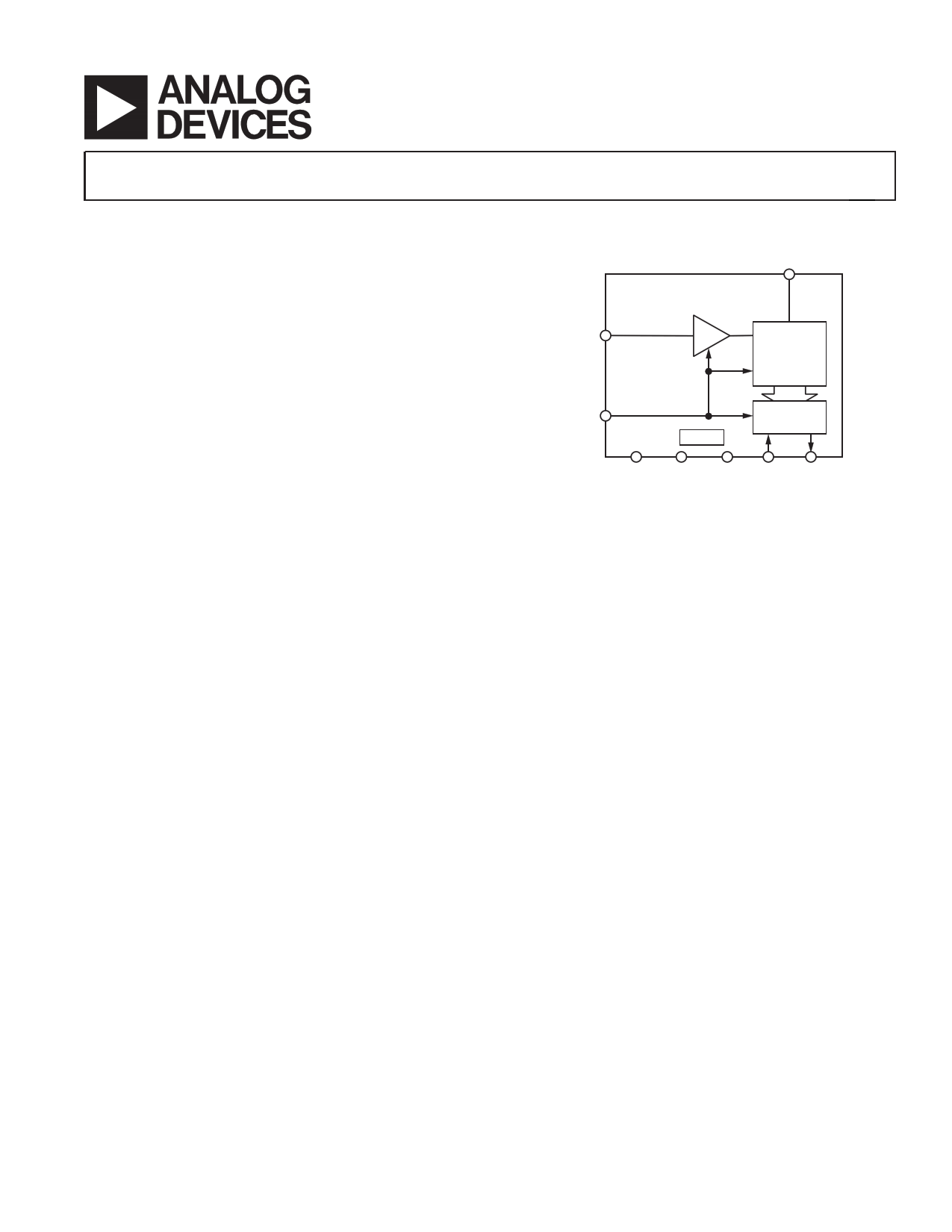
FUNCTIONAL BLOCK DIAGRAM
AD7896
TRACK-AND-HOLD
VIN
VDD
12-BIT
ADC
CONVST
CLOCK
OUTPUT
REGISTER
AGND DGND BUSY SCLK SDATA
GENERAL DESCRIPTION
The AD7896 is a fast, 12-bit ADC that operates from a single
2.7 V to 5.5 V supply and is housed in small 8-lead PDIP and
8-lead SOIC packages. The part contains an 8 µs successive
approximation ADC, an on-chip track-and-hold amplifier, an
on-chip clock, and a high speed serial interface.
Output data from the AD7896 is provided via a high speed,
serial interface port. This 2-wire serial interface has a serial
clock input and a serial data output with the external serial
clock accessing the serial data from the part.
In addition to the traditional dc accuracy specifications, such as
linearity, full-scale, and offset errors, the AD7896 is also speci-
fied for dynamic performance parameters, including harmonic
distortion and signal-to-noise ratio.
The part accepts an analog input range of 0 V to VDD and operates
from a single 2.7 V to 5.5 V supply, consuming only 9 mW
typical. The VDD input is also used as the reference for the part
so that no external reference is required.
The AD7896 features a high sampling rate mode and, for low
power applications, a proprietary automatic power-down mode
where the part automatically goes into power-down once conver-
sion is complete and “wakes up” before the next conversion cycle.
The part is available in a small, 8-lead, 0.3'' wide, plastic or
hermetic dual-in-line package (PDIP) and in an 8-lead, small
outline IC (SOIC).
PRODUCT HIGHLIGHTS
1. Complete, 12-bit ADC in an 8-Lead Package.
The AD7896 contains an 8 µs ADC, a track-and-hold ampli-
fier, control logic, and a high speed serial interface, all in an
8-lead PDIP. The VDD input is used as the reference for the
part, so no external reference is needed. This offers consider-
able space saving over alternative solutions.
2. Low Power, Single-Supply Operation.
The AD7896 operates from a single 2.7 V to 5.5 V supply
and consumes only 9 mW typical. The automatic power-
down mode, where the part goes into power down once
conversion is complete and “wakes up” before the next con-
version cycle, makes the AD7896 ideal for battery-powered
or portable applications.
3. High Speed Serial Interface.
The part provides high speed serial data and serial clock lines
allowing for an easy, 2-wire serial interface arrangement.
Rev. D
Information furnished by Analog Devices is believed to be accurate and
reliable. However, no responsibility is assumed by Analog Devices for its
use, nor for any infringements of patents or other rights of third parties that
may result from its use. No license is granted by implication or otherwise
under any patent or patent rights of Analog Devices. Trademarks and
registered trademarks are the property of their respective companies.
One Technology Way, P.O. Box 9106, Norwood, MA 02062-9106, U.S.A.
Tel: 781/329-4700
www.analog.com
Fax:781/461-3113 ©1994–2011 Analog Device, Inc. All rights reserved.
1 page 
AD7896
ABSOLUTE MAXIMUM RATINGS*
(TA = 25°C, unless otherwise noted.)
VDD to AGND . . . . . . . . . . . . . . . . . . . . . . . . . . –0.3 V to +7 V
VDD to DGND . . . . . . . . . . . . . . . . . . . . . . . . . . –0.3 V to +7 V
Analog Input Voltage to AGND . . . . . . –0.3 V to VDD + 0.3 V
Digital Input Voltage to DGND . . . . . . –0.3 V to VDD + 0.3 V
Digital Output Voltage to DGND . . . . . –0.3 V to VDD + 0.3 V
Operating Temperature Range
Commercial (J Version) . . . . . . . . . . . . . . . . . 0°C to +70°C
Industrial (A, B Versions) . . . . . . . . . . . . . . –40°C to +85°C
Extended (S Version) . . . . . . . . . . . . . . . . . –55°C to +125°C
Storage Temperature Range . . . . . . . . . . . . . –65°C to +150°C
Junction Temperature . . . . . . . . . . . . . . . . . . . . . . . . . . 150°C
PDIP Package, Power Dissipation . . . . . . . . . . . . . . . . 450 mW
JA Thermal Impedance . . . . . . . . . . . . . . . . . . . . . 125°C/W
JC Thermal Impedance . . . . . . . . . . . . . . . . . . . . . . 50°C/W
Lead Temperature (Soldering, 10 sec) . . . . . . . . . . . . 260°C
SOIC Package, Power Dissipation . . . . . . . . . . . . . . . . 450 mW
JA Thermal Impedance . . . . . . . . . . . . . . . . . . . . . 160°C/W
JC Thermal Impedance . . . . . . . . . . . . . . . . . . . . . . 75°C/W
Lead Temperature, Soldering
Vapor Phase (60 sec) . . . . . . . . . . . . . . . . . . . . . . . 215°C
Infrared (15 sec) . . . . . . . . . . . . . . . . . . . . . . . . . . . 220°C
ESD . . . . . . . . . . . . . . . . . . . . . . . . . . . . . . . . . . . . .>4000 V
*Stresses above those listed under Absolute Maximum Ratings may cause perma-
nent damage to the device. This is a stress rating only; functional operation of the
device at these or any other conditions above those listed in the operational
sections of this specification is not implied. Exposure to absolute maximum rating
conditions for extended periods may affect device reliability.
CAUTION
ESD (electrostatic discharge) sensitive device. Electrostatic charges as high as 4000 V readily
accumulate on the human body and test equipment and can discharge without detection. Although the
AD7896 features proprietary ESD protection circuitry, permanent damage may occur on devices
subjected to high energy electrostatic discharges. Therefore, proper ESD precautions are recommended
to avoid performance degradation or loss of functionality.
–4– Rev. D
5 Page 
AD7896
To chip select the AD7896 in systems where more than one
device is connected to the 8X51/L51 serial port, a port bit,
configured as an output, from one of the 8X51/L51 parallel
ports can be used to gate on or off the serial clock to the AD7896.
A simple AND function on this port bit and the serial clock from
the 8X51/L51 will provide this function. The port bit should be
high to select the AD7896 and low when it is not selected.
The end of conversion is monitored by using the BUSY signal,
which is shown in the interface diagram of Figure 5, with the
BUSY line from the AD7896 connected to the Port P1.2 of the
8X51/L51 so the BUSY line can be polled by the 8X51/L51.
The BUSY line can be connected to the INT1 line of the
8X51/L51 if an interrupt driven system is preferred. These two
options are shown on the diagram.
Note also that the AD7896 outputs the MSB first during a read
operation while the 8X51/L51 expects the LSB first. Therefore,
the data that is read into the serial buffer needs to be rearranged
before the correct data format from the AD7896 appears in the
accumulator.
The serial clock rate from the 8X51/L51 is limited to signifi-
cantly less than the allowable input serial clock frequency with
which the AD7896 can operate. As a result, the time to read
data from the part will actually be longer than the conversion
time of the part. This means that the AD7896 cannot run at its
maximum throughput rate when used with the 8X51/L51.
P1.2
OR
INT1
8X51/L51
P3.0
BUSY
AD7896
SDATA
P3.1
SCLK
Figure 5. AD7896 to 8X51/L51 Interface
AD7896–68HC11/L11 Interface
An interface circuit between the AD7896 and the 68HC11/L11
microcontroller is shown in Figure 6. For the interface shown,
the 68HC11/L11 SPI port is used and the 68HC11/L11 is con-
figured in its single-chip mode. The 68HC11/L11 is configured
in the master mode with its CPOL bit set to a Logic 0 and its
CPHA bit set to a Logic 1. As with the previous interface, the
diagram shows the simplest form of the interface, where the
AD7896 is the only part connected to the serial port of the
68HC11/L11 and, therefore, no decoding of the serial read
operations is required.
Once again, to chip select the AD7896 in systems where more
than one device is connected to the 68HC11/L11 serial port, a
port bit, configured as an output, from one of the 68HC11/L11
parallel ports can be used to gate on or off the serial clock to the
AD7896. A simple AND function on this port bit and the serial
clock from the 68HC11/L11 will provide this function. The port
bit should be high to select the AD7896 and low when it is
not selected.
The end of conversion is monitored by using the BUSY signal
which is shown in the interface diagram of Figure 6. With the
BUSY line from the AD7896 connected to the Port PC2 of the
68HC11/L11, the BUSY line can be polled by the 68HC11/L11.
The BUSY line can be connected to the IRQ line of the
68HC11/L11 if an interrupt driven system is preferred. These
two options are shown in the diagram.
The serial clock rate from the 68HC11/L11 is limited to signifi-
cantly less than the allowable input serial clock frequency with
which the AD7896 can operate. As a result, the time to read
data from the part will actually be longer than the conversion
time of the part. This means that the AD7896 cannot run at its
maximum throughput rate when used with the 68HC11/L11.
PC2 OR
IRQ
68HC11/L11
SCK
BUSY
AD7896
SCLK
MISO
SDATA
Figure 6. AD7896 to 68HC11/L11 Interface
AD7896–ADSP-2105 Interface
An interface circuit between the AD7896 and the ADSP-2105 DSP
processor is shown in Figure 7. In the interface shown, the RFS1
output from the ADSP-2105s SPORT1 serial port is used to gate
the serial clock (SCLK1) of the ADSP-2105 before it is applied to
the SCLK input of the AD7896. The RFS1 output is configured for
active high operation. The BUSY line from the AD7896 is
connected to the IRQ2 line of the ADSP-2105 so that at the end of
conversion an interrupt is generated telling the ADSP-2105 to
initiate a read operation. The interface ensures a noncontinuous
clock for the AD7896’s serial clock input, with only 16 serial clock
pulses provided and the serial clock line of the AD7896 remaining
low between data transfers. The SDATA line from the AD7896 is
connected to the DR1 line of the ADSP-2105 serial port.
The timing relationship between the SCLK1 and RFS1 outputs of the
ADSP-2105 are such that the delay between the rising edge of the
SCLK1 and the rising edge of an active high RFS1 is up to 30 ns.
There is also a requirement that data must be set up 10 ns prior to the
falling edge of the SCLK1 to be read correctly by the ADSP-2105.
The data access time for the AD7896 is 60 ns (5 V [A, B versions])
from the rising edge of its SCLK input. Assuming a 10 ns propa-
gation delay through the external AND gate, the high time of the
SCLK1 output of the ADSP-2105 must be ≥ (30 + 60 + 10 + 10) ns,
i.e., ≥110 ns. This means that the serial clock frequency with which
the interface of Figure 7 can work is limited to 4.5 MHz. However,
there is an alternative method that allows for the ADSP-2105 SCLK1
to run at 5 MHz (which is the max serial clock frequency of the
SCLK1 output). The arrangement is where the first leading zero of the
data stream from the AD7896 cannot be guaranteed to be clocked into
the ADSP-2105 due to the combined delay of the RFS signal and the
data access time of the AD7896. In most cases, this is acceptable as
there will still be three leading zeros followed by the 12 data bits.
–10–
Rev. D
11 Page | ||
| Páginas | Total 16 Páginas | |
| PDF Descargar | [ Datasheet AD7896.PDF ] | |
Hoja de datos destacado
| Número de pieza | Descripción | Fabricantes |
| AD7890 | 12-Bit Serial Data Acquisition System | Analog Devices |
| AD7891 | 12-Bit High Speed Data Acquisition System | Analog Devices |
| AD7892 | LC2MOS Single Supply/ 12-Bit 600 kSPS ADC | Analog Devices |
| AD7893 | LC2MOS 12-Bit/ Serial 6 us ADC in 8-Pin Package | Analog Devices |
| Número de pieza | Descripción | Fabricantes |
| SLA6805M | High Voltage 3 phase Motor Driver IC. |
Sanken |
| SDC1742 | 12- and 14-Bit Hybrid Synchro / Resolver-to-Digital Converters. |
Analog Devices |
|
DataSheet.es es una pagina web que funciona como un repositorio de manuales o hoja de datos de muchos de los productos más populares, |
| DataSheet.es | 2020 | Privacy Policy | Contacto | Buscar |