|
|
|
PDF LMR342FVT Data sheet ( Hoja de datos )
| Número de pieza | LMR342FVT | |
| Descripción | Low Supply Current Output Full Swing CMOS Operational Amplifiers | |
| Fabricantes | ROHM Semiconductor | |
| Logotipo | ||
Hay una vista previa y un enlace de descarga de LMR342FVT (archivo pdf) en la parte inferior de esta página. Total 30 Páginas | ||
|
No Preview Available !
Datasheet
Low Supply Current Output Full Swing
CMOS Operational Amplifiers
LMR341G LMR342xxx LMR344xxx
General Description
The LMR341G, LMR342xxx and LMR344xxx are input
ground sense, output full swing operational amplifiers.
They have the features of low operating supply voltage,
low supply current and low input bias current. These are
suitable for sensor amplifier, battery-powered electronic
equipment, battery monitoring and audio pre-amps for
voice. Shutdown function is applied to LMR341G.
Features
Low Operating Supply Voltage
Low Input Bias Current
Low Supply Current
Low Input Offset Voltage
Key Specifications
Operating Supply Voltage (Single Supply):
+2.7V to +5.5V
Supply Current (VDD=2.7V, TA=25°C):
LMR341G(Single)
80µA(Typ)
LMR342xxx(Dual)
200µA(Typ)
LMR344xxx(Quad)
400µA(Typ)
Voltage Gain (RL=2k):
Temperature Range:
103dB(Typ)
-40°C to +85°C
Input Offset Voltage (TA=25°C):
Input Bias Current (TA=25°C):
Turn on time from shutdown:
4mV(Max)
1pA(Typ)
2µS(Typ)
Applications
Sensor Amplifier
Battery Monitoring
Battery-Powered Electronic Equipment
Audio Pre-Amps for Voice
Active Filter
Buffer
Consumer Electronics
Package s
SSOP6
SOP8
SOP-J8
SSOP-B8
TSSOP-B8
MSOP8
TSSOP-B8J
SOP14
SOP-J14
TSSOP-B14J
W(Typ) xD(Typ) xH(Max)
2.90mm x 2.80mm x 1.25mm
5.00mm x 6.20mm x 1.71mm
4.90mm x 6.00mm x 1.65mm
3.00mm x 6.40mm x 1.35mm
3.00mm x 6.40mm x 1.20mm
2.90mm x 4.00mm x 0.90mm
3.00mm x 4.90mm x 1.10mm
8.70mm x 6.20mm x 1.71mm
8.65mm x 6.00mm x 1.65mm
5.00mm x 6.40mm x 1.20mm
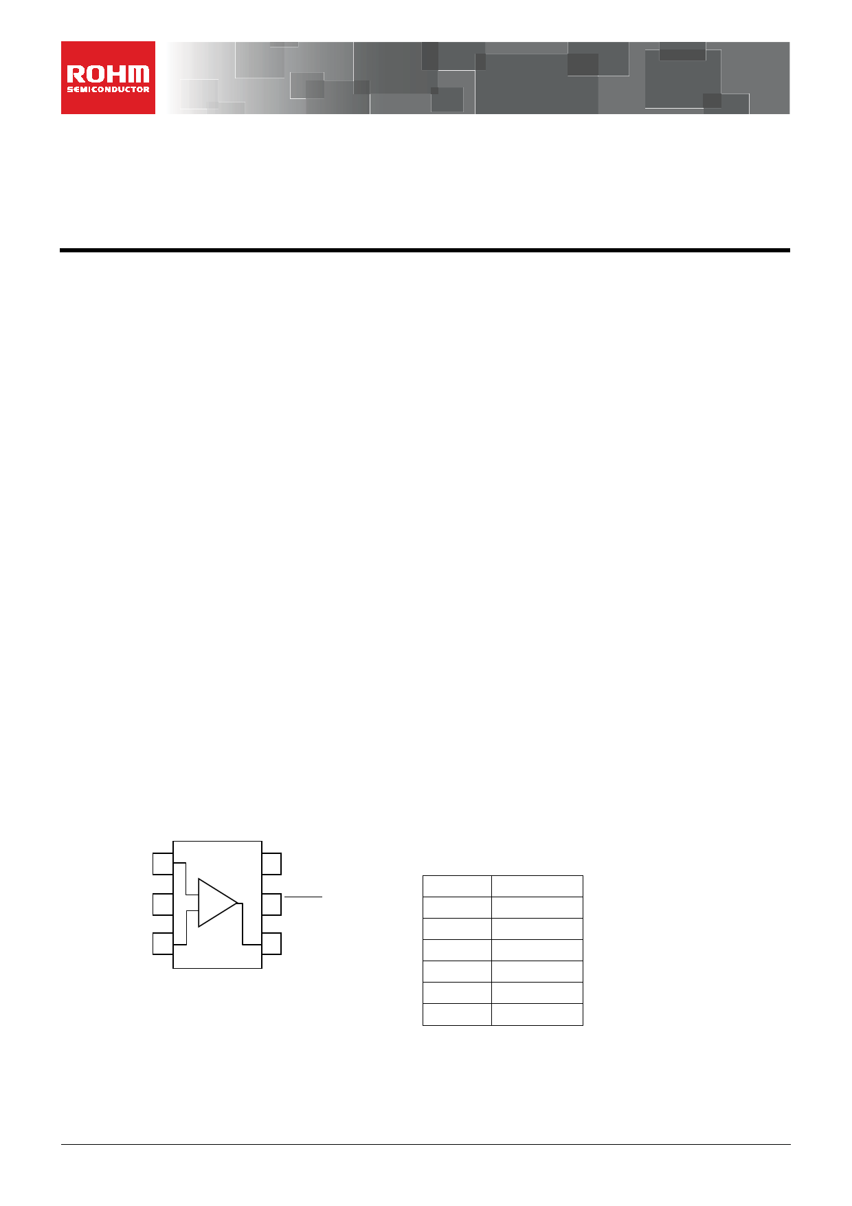
Pin Configuration
LMR341G : SSOP6
5 VDD
4 OUT
+IN 1
VSS 2
-IN 3
+
-
6 VDD
5 SHDN
4 OUT
SSOP6
Pin No.
1
2
3
4
5
6
Pin Name
+IN
VSS
-IN
OUT
——————
SHDN
VDD
○Product structure:Silicon monolithic integrated circuit ○This product has no designed protection against radioactive rays.
www.rohm.com
©2013 ROHM Co., Ltd. All rights reserved.
TSZ22111・14・001
1/50
TSZ02201-0RAR0G200670-1-2
16.Jun.2015 Rev.007
1 page 
LMR341G LMR342xxx LMR344xxx
Datasheet
Electrical Characteristics:
——————
○LMR341G (Unless otherwise specified VDD=+2.7V, VSS=0V, SHDN=VDD)
Parameter
Symbol
Temperature
Range
Min
Limits
Typ
Input Offset Voltage (Note 12,13)
VIO
25°C
Full Range
-
-
0.25
-
Input Offset Voltage Drift
(Note 12,13)
VIO/T Full Range
-
1.7
Max
4
4.5
-
Input Offset Current (Note 12)
IIO 25°C
-
1
-
Input Bias Current (Note 12)
IB 25°C -
1
Supply Current(Note 13)
25°C
IDD Full Range
-
-
80
-
Shutdown Current
IDD_SD 25°C - 0.2
Maximum Output Voltage(High)
Maximum Output Voltage(Low)
Large Signal Voltage Gain
Input Common-Mode
Voltage Range
VOH
VOL
AV
VICM
25°C
25°C
25°C
25°C
VDD-0.06 VDD-0.03
VDD-0.03 VDD-0.01
- 0.03
- 0.01
78 113
72 103
0-
200
170
230
1000
-
-
0.06
0.03
-
-
1.7
Common-Mode Rejection Ratio CMRR
25°C
56
80
-
Power Supply Rejection Ratio
Output Source Current (Note 14)
Output Sink Current (Note 14)
PSRR
ISOURCE
ISINK
25°C
25°C
25°C
65
20
30
82
32
45
-
-
-
Slew Rate
SR 25°C - 1.0 -
Gain Bandwidth
GBW
25°C
-
2.0
-
Unit Gain Frequency
Phase Margin
fT 25°C - 1.2 -
θM 25°C
-
50
-
Gain Margin
Input Referred Noise Voltage
Total Harmonic Distortion
+ Noise
GM
VN
THD+N
25°C
25°C
25°C
- 4.5 -
- 40 -
-3-
- 0.017 -
Turn On Time From Shutdown TON
25°C
-
2
-
Unit Condition
mV -
μV/°C
-
pA -
pA -
μA
RL=∞,
AV=0dB, +IN=VDD/2
nA
_______________
SHDN=GND
V
RL=2kΩ to VDD/2
RL=10kΩ to VDD/2
V
RL=2kΩ to VDD/2
RL=10kΩ to VDD/2
dB
RL=10kΩ to VDD/2
RL=2kΩ to VDD/2
V-
dB VICM=VDD/2
dB
VDD=2.7V to 5.0V
VICM=0.5V
mA OUT=0V, short current
mA
V/μs
MHz
MHz
deg
dB
nV/ Hz
µVrms
%
μs
OUT=2.7V
short current
RL=10kΩ, +IN=1.2VP-P
CL=200pF, RL=100kΩ
AV=40dB, f=100kHz
CL=200pF, RL=100kΩ
AV =40dB, gain=0dB
CL=20pF, RL=100kΩ
AV=40dB
CL=20pF, RL=100kΩ
AV=40dB
f=1kHz, AV=40dB
AV=40dB, DIN-AUDIO
RL=600Ω, AV=0dB
OUT=1VP-P, f=1kHz
DIN-AUDIO
-
Turn On Voltage High
VSHDN_H 25°C - 1.8 -
V
-
Turn On Voltage Low
VSHDN_L 25°C - 1.1 -
V
(Note 12) Absolute value.
(Note 13) Full Range: TA=-40°C to +85°C
(Note 14) Under the high temperature environment, consider the power dissipation of IC when selecting the output current.
When the terminal short circuits are continuously output, the output current is reduced to climb to the temperature inside IC.
-
www.rohm.com
©2013 ROHM Co., Ltd. All rights reserved.
TSZ22111・15・001
5/50
TSZ02201-0RAR0G200670-1-2
16.Jun.2015 Rev.007
5 Page 
LMR341G LMR342xxx LMR344xxx
Datasheet
Description of Electrical Characteristics
Described below are descriptions of the relevant electrical terms used in this datasheet. Items and symbols used are also
shown. Note that item name and symbol and their meaning may differ from those on another manufacturer’s document or
general document.
1. Absolute maximum ratings
Absolute maximum rating items indicate the condition which must not be exceeded. Application of voltage in excess of absolute
maximum rating or use out of absolute maximum rated temperature environment may cause deterioration of characteristics.
(1) Supply Voltage (VDD/VSS)
Indicates the maximum voltage that can be applied between the VDD terminal and VSS terminal without
deterioration or destruction of characteristics of internal circuit.
(2) Differential Input Voltage (VID)
Indicates the maximum voltage that can be applied between non-inverting and inverting terminals without damaging
the IC.
(3) Input Common-Mode Voltage Range (VICM)
Indicates the maximum voltage that can be applied to the non-inverting and inverting terminals without deterioration
or destruction of electrical characteristics. Input common-mode voltage range of the maximum ratings does not assure
normal operation of IC. For normal operation, use the IC within the input common-mode voltage range characteristics.
(4) Power Dissipation (PD)
Indicates the power that can be consumed by the IC when mounted on a specific board at the ambient temperature 25°C
(normal temperature). As for package product, PD is determined by the temperature that can be permitted by the IC in
the package (maximum junction temperature) and the thermal resistance of the package.
2. Electrical characteristics
(1) Input Offset Voltage (VIO)
Indicates the voltage difference between non-inverting terminal and inverting terminals. It can be translated into the
input voltage difference required for setting the output voltage at 0 V.
(2) Input Offset Voltage drift (VIO/T)
Denotes the ratio of the input offset voltage fluctuation to the ambient temperature fluctuation.
(3) Input Offset Current (IIO)
Indicates the difference of input bias current between the non-inverting and inverting terminals.
(4) Input Bias Current (IB)
Indicates the current that flows into or out of the input terminal. It is defined by the average of input bias currents at
the non-inverting and inverting terminals.
(5) Supply Current (IDD)
Indicates the current that flows within the IC under specified no-load conditions.
(6) Shutdown current (IDD_SD)
Indicates the current when the circuit is shutdown.
(7) Maximum Output Voltage(High) / Maximum Output Voltage(Low) (VOH/VOL)
Indicates the voltage range of the output under specified load condition. It is typically divided into maximum output
voltage high and low. Maximum output voltage high indicates the upper limit of output voltage. Maximum output
voltage low indicates the lower limit.
(8) Large Signal Voltage Gain (AV)
Indicates the amplifying rate (gain) of output voltage against the voltage difference between non-inverting terminal
and inverting terminal. It is normally the amplifying rate (gain) with reference to DC voltage.
AV = (Output voltage) / (Differential Input voltage)
(9) Input Common-Mode Voltage Range (VICM)
Indicates the input voltage range where IC normally operates.
(10) Common-Mode Rejection Ratio (CMRR)
Indicates the ratio of fluctuation of input offset voltage when the input common mode voltage is changed. It is
normally the fluctuation of DC.
CMRR = (Change of Input common-mode voltage)/(Input offset fluctuation)
(11) Power Supply Rejection Ratio (PSRR)
Indicates the ratio of fluctuation of input offset voltage when supply voltage is changed.
It is normally the fluctuation of DC.
PSRR = (Change of power supply voltage)/(Input offset fluctuation)
(12) Output Source Current/ Output Sink Current (ISOURCE / ISINK)
The maximum current that can be output from the IC under specific output conditions. The output source current
indicates the current flowing out from the IC, and the output sink current indicates the current flowing into the IC.
(13) Slew Rate (SR)
Indicates the ratio of the change in output voltage with time when a step input signal is applied.
(14) Unity Gain Frequency (fT)
Indicates a frequency where the voltage gain of operational amplifier is 1.
www.rohm.com
©2013 ROHM Co., Ltd. All rights reserved.
TSZ22111・15・001
11/50
TSZ02201-0RAR0G200670-1-2
16.Jun.2015 Rev.007
11 Page | ||
| Páginas | Total 30 Páginas | |
| PDF Descargar | [ Datasheet LMR342FVT.PDF ] | |
Hoja de datos destacado
| Número de pieza | Descripción | Fabricantes |
| LMR342FV | Low Supply Current Output Full Swing CMOS Operational Amplifiers | ROHM Semiconductor |
| LMR342FVJ | Low Supply Current Output Full Swing CMOS Operational Amplifiers | ROHM Semiconductor |
| LMR342FVM | Low Supply Current Output Full Swing CMOS Operational Amplifiers | ROHM Semiconductor |
| LMR342FVT | Low Supply Current Output Full Swing CMOS Operational Amplifiers | ROHM Semiconductor |
| Número de pieza | Descripción | Fabricantes |
| SLA6805M | High Voltage 3 phase Motor Driver IC. |
Sanken |
| SDC1742 | 12- and 14-Bit Hybrid Synchro / Resolver-to-Digital Converters. |
Analog Devices |
|
DataSheet.es es una pagina web que funciona como un repositorio de manuales o hoja de datos de muchos de los productos más populares, |
| DataSheet.es | 2020 | Privacy Policy | Contacto | Buscar |