|
|
|
PDF NCS325 Data sheet ( Hoja de datos )
| Número de pieza | NCS325 | |
| Descripción | Zero-Drift Operational Amplifier | |
| Fabricantes | ON Semiconductor | |
| Logotipo | ||
Hay una vista previa y un enlace de descarga de NCS325 (archivo pdf) en la parte inferior de esta página. Total 15 Páginas | ||
|
No Preview Available !
NCS325, NCS2325,
NCS4325
50 mV Offset, 0.25 mV/5C,
35 mA, Zero-Drift
Operational Amplifier
The NCS325, NCS2325 and NCS4325 are CMOS operational
amplifiers providing precision performance. The Zero−Drift
architecture allows for continuous auto−calibration, which provides
very low offset, near−zero drift over time and temperature, and near
flat 1/f noise at only 35 mA (max) quiescent current. These benefits
make these devices ideal for precision DC applications. These op
amps provide rail−to−rail input and output performance and are
optimized for low voltage operation as low as 1.8 V and up to 5.5 V.
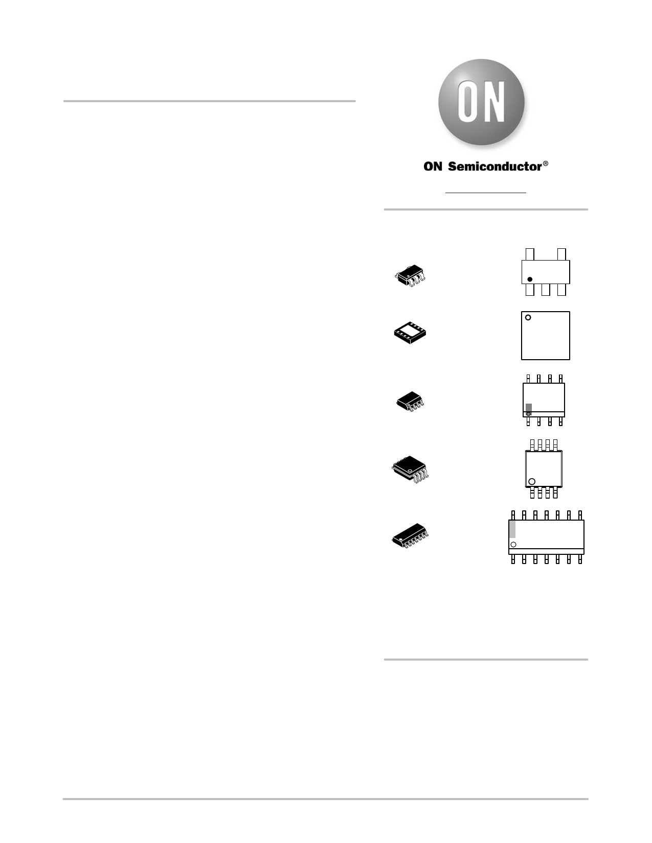
The single channel NCS325 is available in the space−saving SOT23−5
package. The dual channel NCS2325 is available in Micro8, SOIC−8,
and DFN−8. The quad channel NCS4325 is available in SOIC−14.
Features
• Low Offset Voltage: 14 mV typ, 50 mV max at 25°C for NCS325
• Zero Drift: 0.25 mV/°C max
• Low Noise: 1 mVpp, 0.1 Hz to 10 Hz
• Quiescent Current: 21 mA typ, 35 mA max at 25°C
• Supply Voltage: 1.8 V to 5.5 V
• Rail−to−Rail Input and Output
• Internal EMI Filtering
• These Devices are Pb−Free, Halogen Free/BFR Free and are RoHS
Compliant
Typical Applications
• Battery Powered Instruments
• Temperature Measurements
• Transducer Applications
• Electronic Scales
• Medical Instrumentation
• Current Sensing
This document contains information on some products that are still under development.
ON Semiconductor reserves the right to change or discontinue these products without
notice.
www.onsemi.com
MARKING
DIAGRAMS
TSOP−5
5
(SOT23−5)
32A AYWG
SN SUFFIX
G
1
CASE 483
1
DFN−8
1 NCS
MN SUFFIX
2325
1 CASE 506BW ALYWG
G
8
SOIC−8
N2325
D SUFFIX
AYWW
1
CASE 751
G
1
8
MSOP−8
DM SUFFIX
CASE 846A
1
2325
AYWG
G
1
14
SOIC−14
NCS4325G
SUFFIX
AWLYWW
1 CASE 751A
1
A = Assembly Location
Y = Year
WL = Wafer Lot
W or WW = Work Week
G or G = Pb−Free Package
(Note: Microdot may be in either location)
ORDERING INFORMATION
See detailed ordering and shipping information on page 2 of
this data sheet.
© Semiconductor Components Industries, LLC, 2013
October, 2016 − Rev. 3
1
Publication Order Number:
NCS325/D
1 page 
NCS325, NCS2325, NCS4325
12
VS = 5 V
10
VCM = midsupply
TA = 25°C
Sample size = 31
8
6
4
2
0
0
3 6 9 12 15 18 21 24 27
OFFSET VOLTAGE (mV)
Figure 1. Offset Voltage Distribution
30
100
80
60 GAIN
40
Gain, VS = 1.8 V
Gain, VS = 5.5 V
Phase, VS = 1.8 V
Phase, VS = 5.5 V
20
0
−20 PHASE
−40
−60
−80
10
100 1000
10k 100k 1M
FREQUENCY (Hz)
Figure 2. Gain and Phase vs. Frequency
90
60
30
0
−30
−60
−90
−120
−150
−180
100
90
80
70
60
50
40
30
20
10
0
10
TA = 25°C
VS = 1.8 V
VS = 5 V
100 1000
10k
FREQUENCY (Hz)
Figure 3. CMRR vs. Frequency
100k
100
90
80
70
60
50
40
30
20
10
0
10
VS = 5 V
RL = 10 kW
TA = 25°C
VSS
VDD
100 1000
10k 100k
FREQUENCY (Hz)
Figure 4. PSRR vs. Frequency
1M
3
VOH, VS = 5 V
2
1 VOH, VS = 1.8 V
TA = 25°C
0
−1 VOL, VS = 1.8 V
−2 VOL, VS = 5 V
−3
0 1234 5 6 78 9
OUTPUT CURRENT (mA)
Figure 5. Output Voltage Swing vs. Output
Current
10
500
400
VS = 1.8 V
TA = 25°C
300 IIB+
200 IIB−
100
0
−100
−200
−300
−400
−500
−1 −0.8 −0.6 −0.4 −0.2 0 0.2 0.4 0.6 0.8
COMMON MODE VOLTAGE (V)
Figure 6. Input Bias Current vs. Common
Mode Voltage, VS = 1.8 V
1
www.onsemi.com
5
5 Page 
NCS325, NCS2325, NCS4325
PACKAGE DIMENSIONS
NOTE 5
2X 0.10 T
2X 0.20 T B 5 4
1 23
BG
AA
TOP VIEW
TSOP−5
CASE 483−02
ISSUE K
D 5X
0.20 C A B
M
S
K
DETAIL Z
C
0.05
H
SIDE VIEW
C
SEATING
PLANE
DETAIL Z
J
END VIEW
NOTES:
1. DIMENSIONING AND TOLERANCING PER ASME
Y14.5M, 1994.
2. CONTROLLING DIMENSION: MILLIMETERS.
3. MAXIMUM LEAD THICKNESS INCLUDES LEAD FINISH
THICKNESS. MINIMUM LEAD THICKNESS IS THE
MINIMUM THICKNESS OF BASE MATERIAL.
4. DIMENSIONS A AND B DO NOT INCLUDE MOLD
FLASH, PROTRUSIONS, OR GATE BURRS. MOLD
FLASH, PROTRUSIONS, OR GATE BURRS SHALL NOT
EXCEED 0.15 PER SIDE. DIMENSION A.
5. OPTIONAL CONSTRUCTION: AN ADDITIONAL
TRIMMED LEAD IS ALLOWED IN THIS LOCATION.
TRIMMED LEAD NOT TO EXTEND MORE THAN 0.2
FROM BODY.
MILLIMETERS
DIM MIN MAX
A 3.00 BSC
B 1.50 BSC
C 0.90 1.10
D 0.25 0.50
G 0.95 BSC
H 0.01 0.10
J 0.10 0.26
K 0.20 0.60
M 0 _ 10 _
S 2.50 3.00
SOLDERING FOOTPRINT*
0.95
0.037
1.9
0.074
2.4
0.094
1.0
0.039
0.7
0.028
ǒ ǓSCALE 10:1
mm
inches
*For additional information on our Pb−Free strategy and soldering
details, please download the ON Semiconductor Soldering and
Mounting Techniques Reference Manual, SOLDERRM/D.
www.onsemi.com
11
11 Page | ||
| Páginas | Total 15 Páginas | |
| PDF Descargar | [ Datasheet NCS325.PDF ] | |
Hoja de datos destacado
| Número de pieza | Descripción | Fabricantes |
| NCS325 | Zero-Drift Operational Amplifier | ON Semiconductor |
| Número de pieza | Descripción | Fabricantes |
| SLA6805M | High Voltage 3 phase Motor Driver IC. |
Sanken |
| SDC1742 | 12- and 14-Bit Hybrid Synchro / Resolver-to-Digital Converters. |
Analog Devices |
|
DataSheet.es es una pagina web que funciona como un repositorio de manuales o hoja de datos de muchos de los productos más populares, |
| DataSheet.es | 2020 | Privacy Policy | Contacto | Buscar |