|
|
|
PDF AH103 Data sheet ( Hoja de datos )
| Número de pieza | AH103 | |
| Descripción | High Linearity Amplifier | |
| Fabricantes | WJ Communication | |
| Logotipo | ||
Hay una vista previa y un enlace de descarga de AH103 (archivo pdf) en la parte inferior de esta página. Total 6 Páginas | ||
|
No Preview Available !
AH103
High Gain, High Linearity ½ Watt Amplifier
The Communications Edge TM
Product Information
Product Features
• 60 – 2700 MHz
• +27 dBm P1dB
• +46 dBm Output IP3
• 28.5 dB Gain @ 900 MHz
• Excellent ACPR
• MTTF > 100 Years
• SOIC-8 Pkg w/ heat slug
Applications
• Mobile Infrastructure
• W-LAN / ISM / RFID
• MDS / MMDS Infrastructure
Product Description
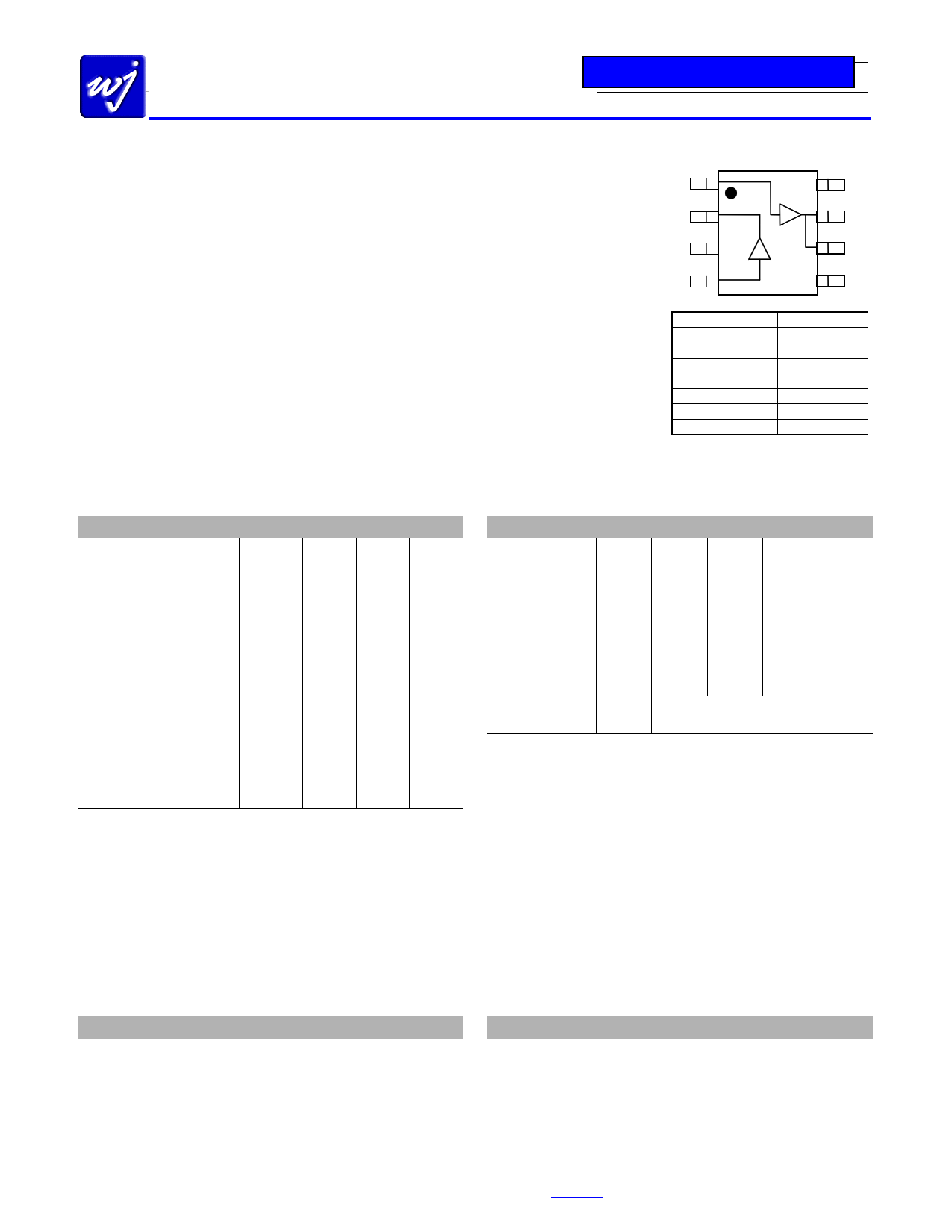
Functional Diagram
The AH103 is a high gain, high linearity ½-Watt
amplifier. This device is comprised of two individual
MMIC amplifiers internally and can be used with an
external interstage match for any of the mobile
infrastructure frequency bands. The dual-stage
amplifier achieves up to +46 dBm IP3 performance
with 28.5 dB gain.
1
2
3 AMP 1
4
AMP 2
8
7
6
5
The device conforms to WJ Communications’ long
history of producing high reliability and quality
components. The AH103 has an associated MTTF of
a minimum of 100 years at a mounting temperature
of 85°C. All devices are 100% RF & DC tested.
The product is targeted for use as driver amplifiers
for wireless infrastructure where high performance
and high linearity are required.
Function
Amp2 in
Amp1 out / Bias 1
Ground
RF in (Amp1 in)
RF out (Amp2 out)
Bias 2
Pin No.
1
2
3, 5, 8,
Backside copper
4
6
7
Specifications
Typical Performance
Parameter
Frequency Range (2)
Gain
Input Return Loss
Output Return Loss
Output P1dB
Output IP3 (3)
IS-95 Channel Power (4)
@ -45 dBc ACPR
Noise Figure
Supply Voltage (Amp1)
Supply Voltage (Amp2)
Operating Current (Amp1)
Operating Current (Amp2)
Thermal Resistance (5)
Junction Temperature (6)
Units
MHz
dB
dB
dB
dBm
dBm
dBm
dB
V
V
mA
mA
°C / W
°C
Min
60
26.5
+26
+43
55
170
Typ
800
28.5
20
11
+27
+46
+21
2.9
+4.5
+9
75
200
Max
2700
100
230
20.6
160
Test conditions unless otherwise noted.
1. T = 25ºC, Vdd1 = +4.5 V, Vdd2 = +9 V, Frequency = 800 MHz in a tuned application circuit.
2. The frequency of operation & bandwidth is determined by the external interstage match.
3. 3OIP measured with two tones at an output power of +10 dBm/tone separated by 10 MHz. The
suppression on the largest IM3 product is used to calculate the 3OIP using a 2:1 rule.
4. IS-95, 9 Channels Forward, Pk/Avg Ratio = 11.5 dB at a .001% probability
±750 kHz offset, 30 kHz BW, Channel BW = 1.23 MHz, frequency = 880 MHz.
5. The worst-case junction temperature for a given ground tab temperature can be calculated by
multiplying the thermal resistance with the total package power dissipation and adding it to the tab
temperature. ie. At 85°C case temperature for a typical device, the worst-case junction temperature
would be = 85°C + (9 V * 0.2 A + 4.5 V * 0.075 A) = 129°C.
6. The junction temperature ensures a minimum MTTF rating of 1 million hours of usage.
Parameter Units
Typical
Frequency
MHz 900 1900 2140 2400
S21
dB 28.5 26
25 24.7
S11 dB -15 -12 -11 -12
S22 dB -11 -11 -14 -17
Output P1dB
dBm +27 +26.5 +26.5 +26
Output IP3
Channel Power
@ -45 dBc ACPR / ACLR
Noise Figure
dBm
dBm
dB
+46
+21
2.9
+45 +45 +43.3
+20 +17.2
3.7 3.5 3.6
Supply Bias 1
+4.5 V @ 75 mA
Supply Bias 2
+9 V @ 200 mA
7. Typical parameters reflect performance in an application circuit.
8. An IS-95 signal is used for 915 / 1960 MHz. A 3GPP W-CDMA signal is used for 2140 MHz.
Absolute Maximum Rating
Ordering Information
Parameter
Operating Case Temperature
Storage Temperature
DC Voltage (pin 2)
DC Voltage (pin 6, 7)
RF Input Power (continuous)
Junction Temperature
Rating
-40 to +85 °C
-55 to +125 °C
+6 V
+11 V
4 dB above Input P1dB
+220°C
Part No.
AH103
AH103-PCB900
AH103-PCB1750
AH103-PCB1900
AH103-PCB2140
Description
High Gain ½ Watt Amplifier
(available in tape and reel)
0.7 – 1.0 GHz Evaluation Circuit
1.7 – 1.8 GHz Evaluation Circuit
1.8 – 2.0 GHz Evaluation Circuit
2.1 – 2.2 GHz Evaluation Circuit
Operation of this device above any of these parameters may cause permanent damage.
Specifications and information are subject to change without notice
WJ Communications, Inc • Phone 1-800-WJ1-4401 • FAX: 408-577-6621 • e-mail: [email protected] • Web site: www.wj.com
November 2003
1 page 
AH103
High Gain, High Linearity ½ Watt Amplifier
Outline Drawing
Mounting Configuration / Land Pattern
The Communications Edge TM
Product Information
Product Marking
The component will be marked with an “AH103”
designator followed by a four- or five-digit alpha-
numeric lot code on the top surface of the
package. Tape and reel specifications for this
part is located on the website in the “Application
Notes” section.
ESD / MSL Information
ESD Classification: Class 1B
Value:
Passes !500 V to <1000 V
Test:
Human Body Model (HBM)
Standard:
JEDEC Standard JESD22-A114
ESD Classification: Class III
Value:
Passes !500 V to <1000 V
Test:
Charged Device Model (CDM)
Standard:
JEDEC Standard JESD22-C101
MSL Rating:
Standard:
Level 1 at +235 °C convection reflow
JEDEC Standard J-STD-020B
Functional Pin Layout
Pin Function
1 Amp2 input
2 Amp1 output / Bias Amp1
3 Ground
4 RF input (Amp1 input)
5 Ground
6 RF output (Amp2 output)
7 Bias Amp2
8 Ground
The backside paddle is the Source and should be
grounded for thermal and electrical purposes. All other
pins should be grounded on the PCB.
Specifications and information are subject to change without notice
WJ Communications, Inc • Phone 1-800-WJ1-4401 • FAX: 408-577-6621 • e-mail: [email protected] • Web site: www.wj.com
November 2003
5 Page | ||
| Páginas | Total 6 Páginas | |
| PDF Descargar | [ Datasheet AH103.PDF ] | |
Hoja de datos destacado
| Número de pieza | Descripción | Fabricantes |
| AH100 | Misch Hexode | TELEFUNKEN |
| AH101 | High Linearity Amplifier | WJ Communication |
| AH101-G | High Linearity Amplifier | TriQuint Semiconductor |
| AH102 | High Linearity Amplifier | WJ Communication |
| Número de pieza | Descripción | Fabricantes |
| SLA6805M | High Voltage 3 phase Motor Driver IC. |
Sanken |
| SDC1742 | 12- and 14-Bit Hybrid Synchro / Resolver-to-Digital Converters. |
Analog Devices |
|
DataSheet.es es una pagina web que funciona como un repositorio de manuales o hoja de datos de muchos de los productos más populares, |
| DataSheet.es | 2020 | Privacy Policy | Contacto | Buscar |