|
|
|
PDF A8601 Data sheet ( Hoja de datos )
| Número de pieza | A8601 | |
| Descripción | Multiple-Output Regulator | |
| Fabricantes | Allegro | |
| Logotipo | ||
Hay una vista previa y un enlace de descarga de A8601 (archivo pdf) en la parte inferior de esta página. Total 30 Páginas | ||
|
No Preview Available !
A8601
Multiple-Output Regulator for Automotive LCD Displays
Features and Benefits
• Automotive Grade AEC-Q100 qualified
• Five individual output supplies
• Independent control of each output voltage
• 350 kHz to 2.25 MHz switching frequency with external
synchronization capability
• <10 μA shutdown current
• Preprogrammed power-up and shutdown sequences
• Overcurrent, overvoltage, short circuit, and thermal
overload protection
Applications:
• GPS
• Infotainment
• Medium LCDs
Package: 28-pin TSSOP with exposed
thermal pad (suffix LP)
Description
The A8601 is a fixed frequency, multiple-output supply for
LCD bias. Its switching frequency can be either programmed
or synchronized with an external clock signal between 350 kHz
and 2.25 MHz, to minimize interference with AM and FM
radio bands.
A total of five output voltages are provided, from three linear
regulators and two charge-pump regulators. Each output
voltage can be adjusted independently. During power-up and
shutdown, the outputs are turned on and off in preprogrammed
sequences, to meet the sequencing requirements for specific
LCD panels.
Short circuit protection is provided for all outputs. The boost
switch is protected against overcurrent and overvoltage. Input
disconnect protection is achieved by driving an external
P-MOSFET.
28-pin exposed thermal pad TSSOP package allows operation
at high ambient temperatures. It is lead (Pb) free with 100%
matte-tin leadframe plating.
Not to scale
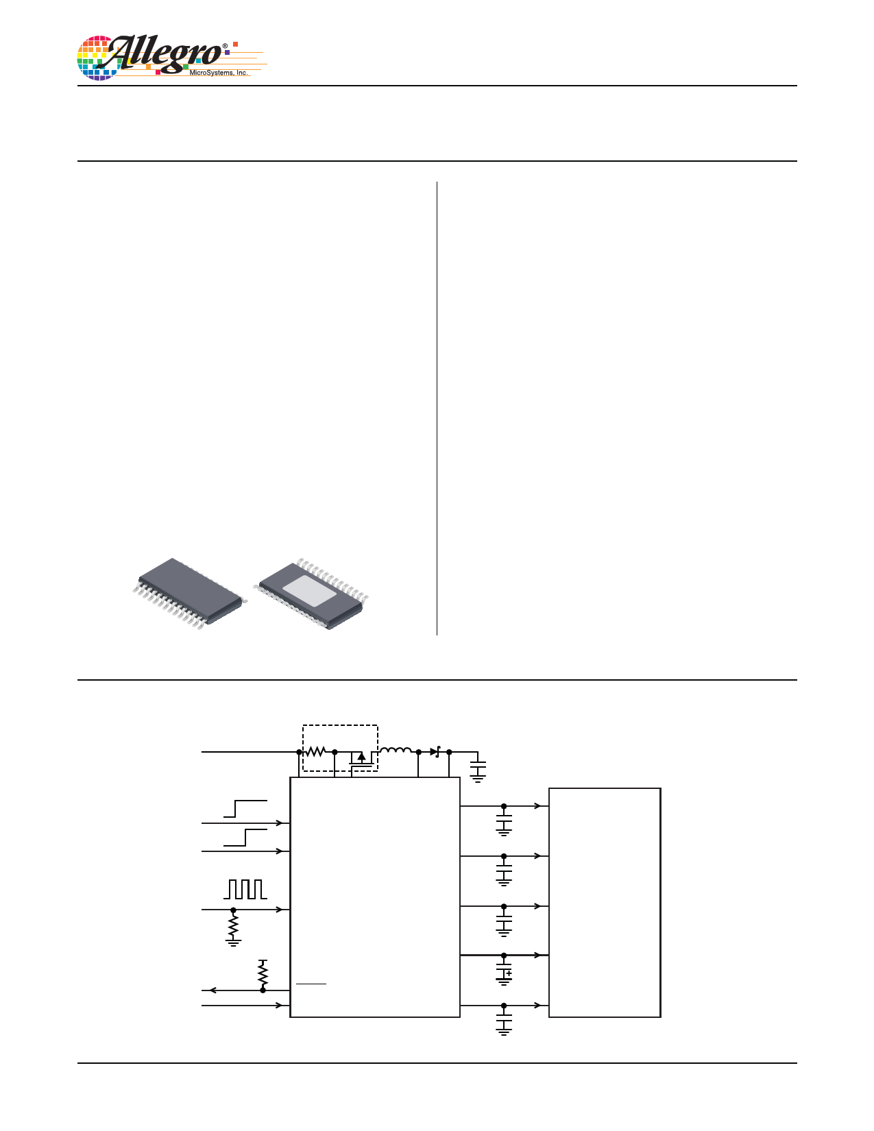
VIN
System Block Diagram
RSCOptionaQl 1
L1
D1
A8601-DS, Rev. 1
External Sync
VIN INS GATE
EN1
A8601
EN2
SW OUT
DVDD
AVDD
VDVDD 3.3 V
VAVDD 5 to 14 V
FSET_SYNC
VVGH 10 to 25 V
VGH
+
LCD Panel
VVIN
VVGL –5 to –12 V
VGL
1.5 to 3.2 V
FAULT
VINAMP
VVCOM 3 to 6 V
VCOM
+
Output voltages shown are
for typical LCD Panel
1 page 
A8601
Multiple-Output Regulator for Automotive LCD Displays
Pin-out Diagram
GATE 1
INS 2
VIN 3
DVDD 4
FB1 5
COMP 6
VINAMP 7
VCOM 8
GNDVCOM 9
FSET_SYNC 10
BIAS 11
FAULT 12
EN1 13
EN2 14
PAD
28 SW
27 PGND
26 OUT
25 AVDD
24 FB2
23 CP11
22 CP12
21 VGH
20 FB4
19 CP21
18 CP22
17 VGL
16 FB3
15 AGND
Terminal List Table
Number
Name
Function
1
GATE
Gate driver for input disconnect P-MOSFET
2
INS
High-side sense for input overcurrent
detection
3 VIN Input supply voltage (4.0 to 5.5 V) for the IC
4
DVDD
Output from internal LDO (item 1 in Functional
Block Diagram) powered by VIN
5
FB1
(DVDD)
Connect to resistor divider network to set
DVDD
6
COMP
Compensation pin, connect to external COMP
capacitor
7 VINAMP Control voltage from external microprocessor
Output from operational amplifier (item 5 in
8 VCOM Functional Block Diagram), controlled by
VINAMP
9 GNDVCOM Ground reference for VCOM
Input for synchronizing boost and charge
pump signals switching frequency to external
10 FSET_SYNC clock signal; alternatively, it can be connected
to an external resistor to set the switching
frequency
11
BIAS
Output from internal 3.6 V bias regulator;
connect to GND via 0.1 μF ceramic capacitor
12 ¯F¯¯A¯¯U¯¯L¯¯T¯ Open-drain output, pulls low in error condition
Enable pin for DVDD output; system can only
13
EN1
be enabled after VVIN is above UVLO level
(refer to Startup Timing Diagram)
Enable pin for the voltage outputs other than
14
EN2
DVDD; it can be activated only after VVIN is
above UVLO and EN1 = high.
Number
15
16
17
18
19
20
21
22
23
24
25
26
27
28
–
Name
AGND
FB3
(VGL)
VGL
CP22
CP21
FB4
(VGH)
VGH
CP12
CP11
FB2
(AVDD)
AVDD
OUT
PGND
SW
PAD
Function
Analog GND reference for signals; connect to
ground plane
Connect to resistor divider network to set VVGL
Inverted charge pump output
(item 3 in Functional Block Diagram)
Capacitor terminal for inverted charge pump
(item 3 in Functional Block Diagram); refer to
Negative Charge Pump section for usage
Capacitor terminal for inverted charge pump
(item 3 in Functional Block Diagram)
Connect to resistor divider network to set VVGH
2x charge pump (item 4 in Functional Block
Diagram) output
Capacitor terminals for charge pump
(item 4 in Functional Block Diagram)
Connect to external resistor network to set
VAVDD
Output from internal LDO (item 2 in Functional
Block Diagram) powered by VOUT
Connect to boost output for internal LDO and
charge pump regulators
Power ground for internal boost switch;
connect this pin to ground terminal of
output ceramic capacitor(s)
Boost converter switch node
Exposed pad (substrate of IC); solder to GND
plane for better thermal conduction
Allegro MicroSystems, Inc.
115 Northeast Cutoff
Worcester, Massachusetts 01615-0036 U.S.A.
1.508.853.5000; www.allegromicro.com
5
5 Page 
A8601
Multiple-Output Regulator for Automotive LCD Displays
VIN
EN1
EN2
DVDD
AVDD
VGL
VGH
VINAMP
VCOM
Startup and Shutdown Sequences (Irregular)
90%
90%
90%
90%
Case 1 (startup)
VIN
EN1
EN2
DVDD
AVDD
VGL
VGH
VINAMP
VCOM
VUVLO
90%
90%
90%
90%
Case 2 (startup)
VIN
EN1
EN2
DVDD
AVDD
VGL
VGH
VINAMP
VCOM
30%
10%
Case 3 (shutdown)
Notes:
• Case 1 (startup). During a startup sequence, if EN2 goes high before EN1 goes high, EN2 is
ignored until EN1 also goes high and DVDD has risen to 90% of its target voltage.
• Case 2 (startup). During a startup sequence, while VIN is below the UVLO level, VUVLO , the IC is
in sleep mode. If either EN1 or EN2 goes high while the IC is still in sleep mode, they are ignored
until VIN exceeds VUVLO .
• Case 3 (shutdown). During a shutdown sequence, if EN1 goes low before EN2 goes low, EN1
is ignored until EN2 also goes low and VGL has fallen to 30% of its target voltage, or the VGL
shutdown time-out interval has expired.
Allegro MicroSystems, Inc.
115 Northeast Cutoff
Worcester, Massachusetts 01615-0036 U.S.A.
1.508.853.5000; www.allegromicro.com
11
11 Page | ||
| Páginas | Total 30 Páginas | |
| PDF Descargar | [ Datasheet A8601.PDF ] | |
Hoja de datos destacado
| Número de pieza | Descripción | Fabricantes |
| A8600 | Quadruple Output Regulator | Allegro MicroSystems |
| A8600 | WHITE LED BACKLIGHT DRIVER SIX-STRING | AiT Semiconductor |
| A8600EJPTR-T | Quadruple Output Regulator | Allegro MicroSystems |
| A8601 | Multiple-Output Regulator | Allegro |
| Número de pieza | Descripción | Fabricantes |
| SLA6805M | High Voltage 3 phase Motor Driver IC. |
Sanken |
| SDC1742 | 12- and 14-Bit Hybrid Synchro / Resolver-to-Digital Converters. |
Analog Devices |
|
DataSheet.es es una pagina web que funciona como un repositorio de manuales o hoja de datos de muchos de los productos más populares, |
| DataSheet.es | 2020 | Privacy Policy | Contacto | Buscar |