|
|
|
PDF BD9E301EFJ-LB Data sheet ( Hoja de datos )
| Número de pieza | BD9E301EFJ-LB | |
| Descripción | Single Synchronous Buck DC/DC Converter | |
| Fabricantes | ROHM Semiconductor | |
| Logotipo | ||
Hay una vista previa y un enlace de descarga de BD9E301EFJ-LB (archivo pdf) en la parte inferior de esta página. Total 30 Páginas | ||
|
No Preview Available !
Datasheet
7.0V to 36V Input, 2.5A Integrated MOSFET
Single Synchronous Buck DC/DC Converter
BD9E301EFJ-LB
General Description
This is the product guarantees long time support in
Industrial market.
BD9E301EFJ-LB is a synchronous buck switching regulator
with built-in power MOSFETs. It is capable of an output
current of up to 2.5A. It is a current mode control DC/DC
converter and features high-speed transient response.
Phase compensation can also be set easily.
Features
Long Time Support Product for Industrial
Applications.
Synchronous single DC/DC converter.
Over-Current Protection.
Short Circuit Protection.
Thermal Shutdown Protection.
Undervoltage Lockout Protection.
Soft Start.
HTSOP-J8 package (Exposed Pad).
Key Specifications
Input Voltage Range:
7.0V to 36V
Output Voltage Range:
1.0V to VIN×0.7V
Output Current:
2.5A (Max)
Switching Frequency:
570kHz (Typ)
High-Side MOSFET ON-Resistance: 170mΩ (Typ)
Low-Side MOSFET ON-Resistance: 140mΩ (Typ)
Standby Current:
0μA (Typ)
Package
HTSOP-J8
W (Typ) x D (Typ) x H (Max)
4.90mm x 6.00mm x 1.00mm
Applications
Industrial Equipment.
Power supply for FA’s industrial device using 24V
bass.
Consumer applications such as home appliance.
Distribution type power supply system for 12V, and
24V.
HTSOP-J8
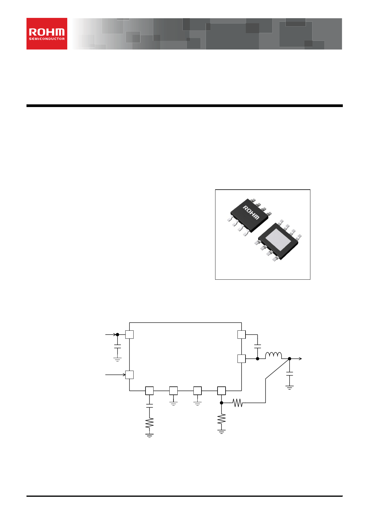
Typical Application Circuit
VIN
24V
10μF
Enable
2 VIN
BD9E301EFJ-LB BOOT 1
3 EN
COMP
6
AGND
4
PGND
7
15kΩ
4700pF
SW 8
FB
5 12kΩ
3kΩ
0.1μF
6.8μH
VOUT
22μF×2
Figure 1. Application circuit
○Product structure:Silicon monolithic integrated circuit.
www.rohm.com
© 2013 ROHM Co., Ltd. All rights reserved.
TSZ22111・14・001
○This product has no designed protection against radioactive rays.
1/30
TSZ02201-0J3J0AJ00380-1-2
14.May.2014 Rev.003
1 page 
BD9E301EFJ-LB
Absolute Maximum Ratings (Ta = 25°C)
Parameter
Symbol
Rating
Unit
Supply Voltage
VIN
-0.3 to +40
V
EN Input Voltage
VEN -0.3 to +40 V
Voltage from GND to BOOT
VBOOT
-0.3 to +45
V
Voltage from SW to BOOT
⊿VBOOT
-0.3 to +7
V
FB Input Voltage
VFB
-0.3 to +7
V
COMP Input Voltage
VCOMP
-0.3 to +7
V
SW Input Voltage
Allowable Power Dissipation
VSW
Pd
-0.5 to VIN + 0.3
3.75 (Note 1)
V
W
Operating Junction Temperature Range
Tj
-40 to +150
C
Storage Temperature Range
Tstg
-55 to +150
C
(Note 1) Derating in done 30.08 mW/°C for operating above Ta≧25°C (Mount on 4-layer 70.0mm x 70.0mm x 1.6mm board)
Caution1: Operating the IC over the absolute maximum ratings may damage the IC. The damage can either be a short circuit between pins or an open circuit
between pins and the internal circuitry. Therefore, it is important to consider circuit protection measures, such as adding a fuse, in case the IC is operated over
the absolute maximum ratings.
Caution2: Reliability is decreased at junction temperature greater than 125C.
Recommended Operating Conditions
Parameter
Rating
Symbol
Min
Typ
Max Unit
Supply Voltage
VIN 7.0 - 36 V
Output Current
IOUT
0
- 2.5 A
Output Voltage Range
VRANGE
1.0(Note 2)
-
VIN × 0.7
V
(Note 2) Please use it in I/O voltage setting of which output pulse width does not become 150nsec (Typ) or less. See the page 22 for how to calculate the
resistance of the output voltage setting.
Electrical Characteristics (Unless otherwise specified VIN=24V VEN=3V Ta=25°C)
Parameter
Symbol
Min
Limit
Typ
Max
Unit
Supply Current in Operating
IOPR - 1.5 2.5 mA
Supply Current in Standby
ISTBY - 0 10 µA
Conditions
VFB = 1.1V
No switching
VEN = 0V
Reference Voltage
VFB 0.98 1.00 1.02 V
FB Input Current
IFB -1 0 1 µA VFB = 0V
Switching frequency
FOSC 484 570 656 kHz
Maximum Duty ratio
Maxduty
85
90
95 %
High-side FET on-resistance
RONH - 170 - mΩ ISW = 100mA
Low-side FET on-resistance
RONL - 140 - mΩ ISW = 100mA
Over Current limit
ILIMIT - 5.0 - A
UVLO detection voltage
VUVLO
6.1
6.4
6.7
V VIN falling
UVLO hysteresis voltage
VUVLOHYS
100
200
300 mV
EN high-level input voltage
VENH
2.5
-
VIN V
EN low-level input voltage
VENL
-
- 0.8 V
EN Input current
IEN
Soft Start time
● VFB : FB Input Voltage. VEN : EN Input Voltage.
● Pd should not be exceeded.
TSS
2.1 4.2 8.4 µA VEN = 3V
1.5
3.0
6.0
msec
EN rising to
FB=0.85V
www.rohm.co
© 2013 ROHM Co., Ltd. All rights reserved.
TSZ22111•15•001
5/30
TSZ02201-0J3J0AJ00380-1-2
14.May.2014 Rev.003
5 Page 
BD9E301EFJ-LB
Typical Performance Curves - continued
VIN=10V/div
EN=10V/div
Time=1ms/div
VOUT=2V/div
SW=10V/div
Figure 21. Power Up (VIN = EN)
(VOUT = 5.0V)
Time=1ms/div
VIN=10V/div
EN=10V/div
VOUT=2V/div
SW=10V/div
Figure 22. Power Down (VIN = EN)
(VOUT = 5.0V)
VIN=10V/div
EN=2V/div
VOUT=2V/div
Time=1ms/div
Time=1ms/div
VIN=10V/div
EN=2V/div
VOUT=2V/div
SW=10V/div
Figure 23. Power Up (EN = 0V→5V)
(VOUT = 5.0V)
SW=10V/div
Figure 24. Power Down (EN = 5V→0V)
(VOUT = 5.0V)
www.rohm.co
© 2013 ROHM Co., Ltd. All rights reserved.
TSZ22111•15•001
11/30
TSZ02201-0J3J0AJ00380-1-2
14.May.2014 Rev.003
11 Page | ||
| Páginas | Total 30 Páginas | |
| PDF Descargar | [ Datasheet BD9E301EFJ-LB.PDF ] | |
Hoja de datos destacado
| Número de pieza | Descripción | Fabricantes |
| BD9E301EFJ-LB | Single Synchronous Buck DC/DC Converter | ROHM Semiconductor |
| Número de pieza | Descripción | Fabricantes |
| SLA6805M | High Voltage 3 phase Motor Driver IC. |
Sanken |
| SDC1742 | 12- and 14-Bit Hybrid Synchro / Resolver-to-Digital Converters. |
Analog Devices |
|
DataSheet.es es una pagina web que funciona como un repositorio de manuales o hoja de datos de muchos de los productos más populares, |
| DataSheet.es | 2020 | Privacy Policy | Contacto | Buscar |