|
|
PDF 9DBV0941 Data sheet ( Hoja de datos )
| Número de pieza | 9DBV0941 | |
| Descripción | 9-output 1.8V HCSL Fanout Buffer | |
| Fabricantes | IDT | |
| Logotipo |  |
|
Hay una vista previa y un enlace de descarga de 9DBV0941 (archivo pdf) en la parte inferior de esta página. Total 18 Páginas | ||
|
No Preview Available !
9-output 1.8V HCSL Fanout Buffer
w/Zo=100ohms
9DBV0941
DATASHEET
Description
The 9DBV0941 is a member of IDT's Full-Featured PCIe
family. The device has 9 output enables for clock
management, and 3 selectable SMBus addresses. It has
integrated terminations for direct connection to 100ohm
transmission lines.
Recommended Application
PCIe Gen1-3 clock distribution in Storage, Networking,
Compute, Consumer
Output Features
• 9 - 1-200MHz Low-Power (LP) HCSL DIF pairs w/ZO=100
• Easy AC-coupling to other logic families, see IDT
application note AN-891
Key Specifications
• Additive cycle-to-cycle jitter <5ps
• Output-to-output skew < 60ps
• Additive phase jitter is <100fs rms for PCIe Gen3
• Additive phase jitter <300fs rms (12kHz-20MHz @125MHz)
Block Diagram
Features/Benefits
• 100ohm direct connect; saves 36 resistors and 62mm2
compared to standard HCSL
• 53mW typical power consumption; eliminates thermal
concerns
• Outputs can optionally be supplied from any voltage
between 1.05V and 1.8V; maximum power savings
• OE# pins; support DIF power management
• HCSL-compatible differential input; can be driven by
common clock sources
• SMBus-selectable features allow optimization to customer
requirements
• Slew rate for each output; allows tuning for various line
lengths
• Differential output amplitude; allows tuning for various
application environments
• 1MHz to 200MHz operating frequency
• 3.3V tolerant SMBus interface works with legacy controllers
• Selectable SMBus addresses; multiple devices can easily
share an SMBus segment
• Device contains default configuration; SMBus interface not
required for device operation
• Space saving 48-pin 6x6mm VFQFPN; minimal board
space
vOE(8:0)#
9
CLK_IN
CLK_IN#
vSADR
^CKPWRGD_PD#
SDATA_3.3
SCLK_3.3
CONTROL
LOGIC
DIF8
DIF7
DIF6
DIF5
DIF4
DIF3
DIF2
DIF1
DIF0
9DBV0941 REVISION C 03/28/16 1 ©2016 Integrated Device Technology, Inc.
1 page 
9DBV0941 DATASHEET
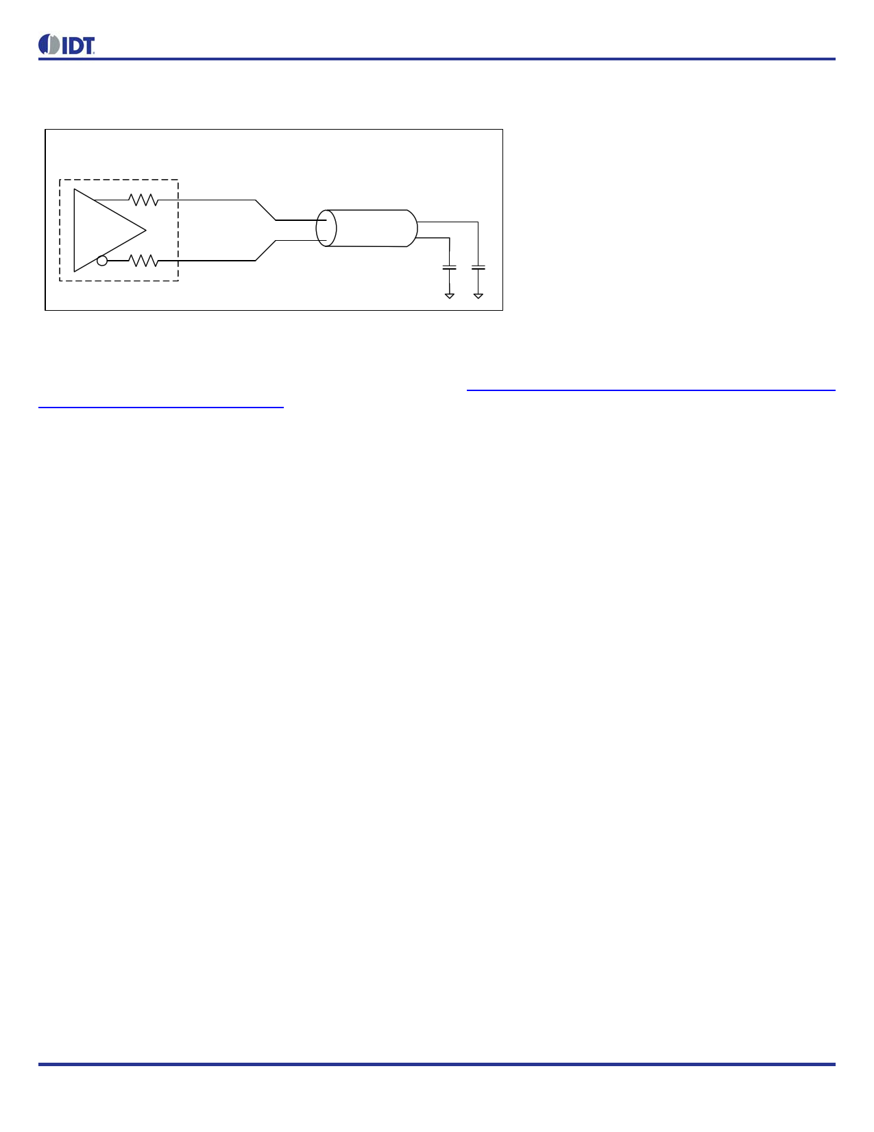
Test Loads
Low-Power HCSL Differential Output Test Load
5 inches
Rs Zo=100W
Rs
Device
2pF 2pF
Alternate Terminations
The 9DBV0941 can easily drive LVPECL, LVDS, and CML logic. See “AN-891 Driving LVPECL, LVDS, and CML Logic with IDT's
"Universal" Low-Power HCSL Outputs” for details.
REVISION C 03/28/16
5 9-OUTPUT 1.8V HCSL FANOUT BUFFER W/ZO=100OHMS
5 Page 
9DBV0941 DATASHEET
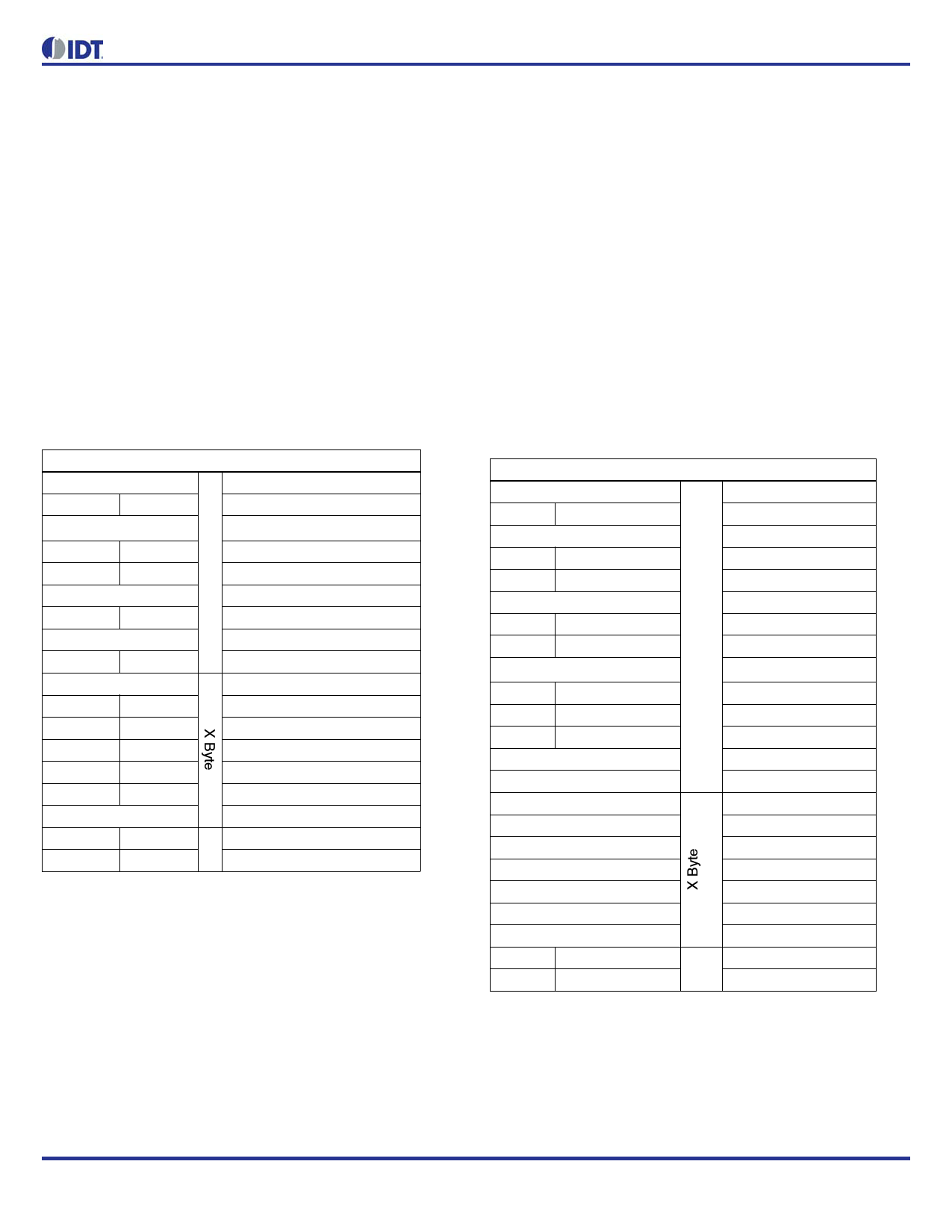
General SMBus Serial Interface Information
How to Write
• Controller (host) sends a start bit
• Controller (host) sends the write address
• IDT clock will acknowledge
• Controller (host) sends the beginning byte location = N
• IDT clock will acknowledge
• Controller (host) sends the byte count = X
• IDT clock will acknowledge
• Controller (host) starts sending Byte N through Byte
N+X-1
• IDT clock will acknowledge each byte one at a time
• Controller (host) sends a Stop bit
Index Block Write Operation
Controller (Host)
IDT (Slave/Receiver)
T starT bit
Slave Address
WR WRite
ACK
Beginning Byte = N
ACK
Data Byte Count = X
ACK
Beginning Byte N
ACK
O
OO
OO
O
Byte N + X - 1
ACK
P stoP bit
Note: SMBus Address is Latched on SADR pin.
How to Read
• Controller (host) will send a start bit
• Controller (host) sends the write address
• IDT clock will acknowledge
• Controller (host) sends the beginning byte location = N
• IDT clock will acknowledge
• Controller (host) will send a separate start bit
• Controller (host) sends the read address
• IDT clock will acknowledge
• IDT clock will send the data byte count = X
• IDT clock sends Byte N+X-1
• IDT clock sends Byte 0 through Byte X (if X(H) was
written to Byte 8)
• Controller (host) will need to acknowledge each byte
• Controller (host) will send a not acknowledge bit
• Controller (host) will send a stop bit
Index Block Read Operation
Controller (Host)
T starT bit
IDT (Slave/Receiver)
Slave Address
WR WRite
ACK
Beginning Byte = N
ACK
RT Repeat starT
Slave Address
RD ReaD
ACK
ACK
ACK
O
O
O
N Not acknowledge
P stoP bit
Data Byte Count=X
Beginning Byte N
O
O
O
Byte N + X - 1
REVISION C 03/28/16
11 9-OUTPUT 1.8V HCSL FANOUT BUFFER W/ZO=100OHMS
11 Page | ||
| Páginas | Total 18 Páginas | |
| PDF Descargar | [ Datasheet 9DBV0941.PDF ] | |
Hoja de datos destacado
| Número de pieza | Descripción | Fabricantes |
| 9DBV0941 | 9-output 1.8V HCSL Fanout Buffer | IDT |
| Número de pieza | Descripción | Fabricantes |
| SLA6805M | High Voltage 3 phase Motor Driver IC. |
Sanken |
| SDC1742 | 12- and 14-Bit Hybrid Synchro / Resolver-to-Digital Converters. |
Analog Devices |
|
DataSheet.es es una pagina web que funciona como un repositorio de manuales o hoja de datos de muchos de los productos más populares, |
| DataSheet.es | 2020 | Privacy Policy | Contacto | Buscar |
