|
|
|
PDF N24C32 Data sheet ( Hoja de datos )
| Número de pieza | N24C32 | |
| Descripción | 32 Kb I2C CMOS Serial EEPROM | |
| Fabricantes | ON Semiconductor | |
| Logotipo | ||
Hay una vista previa y un enlace de descarga de N24C32 (archivo pdf) en la parte inferior de esta página. Total 10 Páginas | ||
|
No Preview Available !
N24C32
32 Kb I2C CMOS Serial
EEPROM
Description
The N24C32 is a 32 Kb CMOS Serial EEPROM device, organized
internally as 128 pages of 32 bytes each. This device supports the
Standard (100 kHz), Fast (400 kHz) and Fast−Plus (1 MHz) I2C
protocol.
Data is written by providing a starting address, then loading 1 to 32
contiguous bytes into a Page Write Buffer, and then writing all data to
non−volatile memory in one internal write cycle. Data is read by
providing a starting address and then shifting out data serially while
automatically incrementing the internal address count.
External address pins make it possible to address up to eight
N24C32 devices on the same bus.
Features
• Supports Standard, Fast and Fast−Plus I2C Protocol
• 1.7 V / 1.6 V to 5.5 V Supply Voltage Range
• 32−Byte Page Write Buffer
• Fast Write Time (4 ms max)
• Hardware Write Protection for Entire Memory
• Schmitt Triggers and Noise Suppression Filters on I2C Bus Inputs
(SCL and SDA)
• Low Power CMOS Technology
• 1,000,000 Program/Erase Cycles
• 100 Year Data Retention
• Industrial and Automotive Grade 1 Temperature Range
• US 8−lead Package
• These Devices are Pb−Free, Halogen Free/BFR Free, and RoHS
Compliant
www.onsemi.com
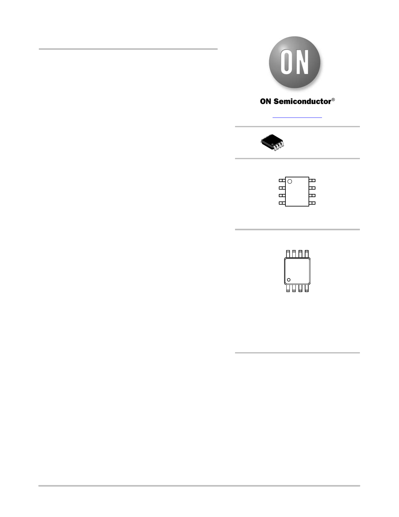
US8
U SUFFIX
CASE 493
PIN CONFIGURATIONS
A0
A1
A2
VSS
1
VCC
WP
SCL
SDA
US8 (U)
(Top View)
MARKING DIAGRAM
8
XX MG
G
1
XX = Specific Device Code*
M = Date Code
G = Pb−Free Package
(Note: Microdot may be in either location)
* See Ordering Information section for the
Specific Device Marking Code
ORDERING INFORMATION
See detailed ordering, marking and shipping information in the
package dimensions section on page 10 of this data sheet.
© Semiconductor Components Industries, LLC, 2016
June, 2016 − Rev. 1
1
Publication Order Number:
N24C32/D
1 page 
N24C32
Power-On Reset (POR)
Each N24C32 incorporates Power-On Reset (POR)
circuitry which protects the internal logic against powering
up in the wrong state. The device will power up into Standby
mode after VCC exceeds the POR trigger level and will
power down into Reset mode when VCC drops below the
POR trigger level. This bi-directional POR behavior
protects the device against ‘brown-out’ failure following a
temporary loss of power.
Pin Description
SCL: The Serial Clock input pin accepts the clock signal
generated by the Master.
SDA: The Serial Data I/O pin accepts input data and delivers
output data. In transmit mode, this pin is open drain. Data is
acquired on the positive edge, and is delivered on the
negative edge of SCL.
A0, A1 and A2: The Address inputs set the device address
that must be matched by the corresponding Slave address
bits. The Address inputs are hard-wired HIGH or LOW
allowing for up to eight devices to be used (cascaded) on the
same bus. When left floating, these inputs are pulled LOW
internally.
WP: When pulled HIGH, the Write Protect input pin
inhibits all write operations. When left floating, this pin is
pulled LOW internally.
Functional Description
The N24C32 supports the Inter-Integrated Circuit (I2C)
Bus protocol. The protocol relies on the use of a Master
device, which provides the clock and directs bus traffic, and
Slave devices which execute requests. The N24C32
operates as a Slave device. Both Master and Slave can
transmit or receive, but only the Master can assign those
roles.
I2C Bus Protocol
The 2-wire I2C bus consists of two lines, SCL and SDA,
connected to the VCC supply via pull-up resistors. The
Master provides the clock to the SCL line, and either the
Master or the Slaves drive the SDA line. A ‘0’ is transmitted
by pulling a line LOW and a ‘1’ by letting it stay HIGH. Data
transfer may be initiated only when the bus is not busy (see
A.C. Characteristics). During data transfer, SDA must
remain stable while SCL is HIGH.
START/STOP Condition
An SDA transition while SCL is HIGH creates a START
or STOP condition (Figure 2). The START consists of a
HIGH to LOW SDA transition, while SCL is HIGH. Absent
the START, a Slave will not respond to the Master. The
STOP completes all commands, and consists of a LOW to
HIGH SDA transition, while SCL is HIGH.
Device Addressing
The Master addresses a Slave by creating a START
condition and then broadcasting an 8-bit Slave address. For
the N24C32, the first four bits of the Slave address are set to
1010 (Ah); the next three bits, A2, A1 and A0, must match
the logic state of the similarly named input pins. The R/W
bit tells the Slave whether the Master intends to read (1) or
write (0) data (Figure 3).
Acknowledge
During the 9th clock cycle following every byte sent to the
bus, the transmitter releases the SDA line, allowing the
receiver to respond. The receiver then either acknowledges
(ACK) by pulling SDA LOW, or does not acknowledge
(NoACK) by letting SDA stay HIGH (Figure 4). Bus timing
is illustrated in Figure 5.
SCL
SDA
START
CONDITION
Figure 2. Start/Stop Timing
STOP
CONDITION
1 0 1 0 A2 A1 A0 R/W
DEVICE ADDRESS
Figure 3. Slave Address Bits
www.onsemi.com
5
5 Page | ||
| Páginas | Total 10 Páginas | |
| PDF Descargar | [ Datasheet N24C32.PDF ] | |
Hoja de datos destacado
| Número de pieza | Descripción | Fabricantes |
| N24C32 | 32 Kb I2C CMOS Serial EEPROM | ON Semiconductor |
| Número de pieza | Descripción | Fabricantes |
| SLA6805M | High Voltage 3 phase Motor Driver IC. |
Sanken |
| SDC1742 | 12- and 14-Bit Hybrid Synchro / Resolver-to-Digital Converters. |
Analog Devices |
|
DataSheet.es es una pagina web que funciona como un repositorio de manuales o hoja de datos de muchos de los productos más populares, |
| DataSheet.es | 2020 | Privacy Policy | Contacto | Buscar |