|
|
PDF EM638165 Data sheet ( Hoja de datos )
| Número de pieza | EM638165 | |
| Descripción | 4M x 16 bit Synchronous DRAM | |
| Fabricantes | Etron Technology | |
| Logotipo |  |
|
Hay una vista previa y un enlace de descarga de EM638165 (archivo pdf) en la parte inferior de esta página. Total 30 Páginas | ||
|
No Preview Available !
EtronTech
EM638165
4M x 16 bit Synchronous DRAM (SDRAM)
Preliminary (Rev. 5.3, Dec. /2013)
Features
Overview
• Fast access time from clock: 4.5/5.4/5.4 ns
• Fast clock rate: 200/166/143 MHz
• Fully synchronous operation
• Internal pipelined architecture
• 1M word x 16-bit x 4-bank
• Programmable Mode registers
- CAS Latency: 2 or 3
- Burst Length: 1, 2, 4, 8, or full page
- Burst Type: Sequential or Interleaved
- Burst stop function
- Optional drive strength control
• Auto Refresh and Self Refresh
• 4096 refresh cycles/64ms
• CKE power down mode
• Single +3.3V ± 0.3V power supply
• Operating Temperature: TA = 0~70°C
• Interface: LVTTL
• 54-pin 400 mil plastic TSOP II package
- Pb and Halogen Free
• 54-ball 8.0 x 8.0 x 1.2mm (max) FBGA package
- Pb free and Halogen free
The EM638165 SDRAM is a high-speed CMOS
synchronous DRAM containing 64 Mbits. It is
internally configured as 4 Banks of 1M word x 16
DRAM with a synchronous interface (all signals are
registered on the positive edge of the clock signal,
CLK). Read and write accesses to the SDRAM are
burst oriented; accesses start at a selected location
and continue for a programmed number of locations
in a programmed sequence. Accesses begin with the
registration of a Bank Activate command which is
then followed by a Read or Write command.
The EM638165 provides for programmable Read
or Write burst lengths of 1, 2, 4, 8, or full page, with a
burst termination option. An auto precharge function
may be enabled to provide a self-timed row precharge
that is initiated at the end of the burst sequence. The
refresh functions, either Auto or Self Refresh are easy
to use. By having a programmable mode register, the
system can choose the most suitable modes to
maximize its performance. These devices are well
suited for applications requiring high memory
bandwidth and particularly well suited to high
performance PC applications.
Table1. Key Specifications
EM638165
tCK3 Clock Cycle time(min.)
tAC3 Access time from CLK(max.)
tRAS Row Active time(min.)
tRC Row Cycle time(min.)
- 5/6/7
5/6/7 ns
4.5/5.4/5.4 ns
40/42/42 ns
55/60/63 ns
Table 2. Ordering Information
Part Number
Frequency
Package
EM638165TS -5G 200MHz
TSOP II
EM638165TS -6G 166MHz
TSOP II
EM638165TS -7G 143MHz
TSOP II
EM638165BM -5H 200MHz
FBGA
EM638165BM -6H 166MHz
FBGA
EM638165BM -7H 143MHz
FBGA
TS: indicates TSOPII Package
BM: indicates FBGA package
G: indicates Pb and Halogen Free for TSOPII Package
H: indicates Pb free and Halogen free
Etron Technology, Inc.
No. 6, Technology Rd. V, Hsinchu Science Park, Hsinchu, Taiwan 30078, R.O.C.
TEL: (886)-3-5782345 FAX: (886)-3-5778671
Etron Technology, Inc. reserves the right to change products or specification without notice.
1 page 
EtronTech
EM638165
LDQM,
UDQM
DQ0-DQ15
NC/RFU
VDDQ
VSSQ
VDD
VSS
Input Data Input/Output Mask: Controls output buffers in read mode and masks
Input data in write mode.
Input / Data I/O: The DQ0-15 input and output data are synchronized with the positive
Output edges of CLK. The I/Os are maskable during Reads and Writes.
- No Connect: These pins should be left unconnected.
Supply DQ Power: Provide isolated power to DQs for improved noise immunity.
( 3.3V± 0.3V )
Supply DQ Ground: Provide isolated ground to DQs for improved noise immunity.
(0V)
Supply Power Supply: +3.3V ± 0.3V
Supply Ground
Rev. 5.3
5
Dec. /2013
5 Page 
EtronTech
EM638165
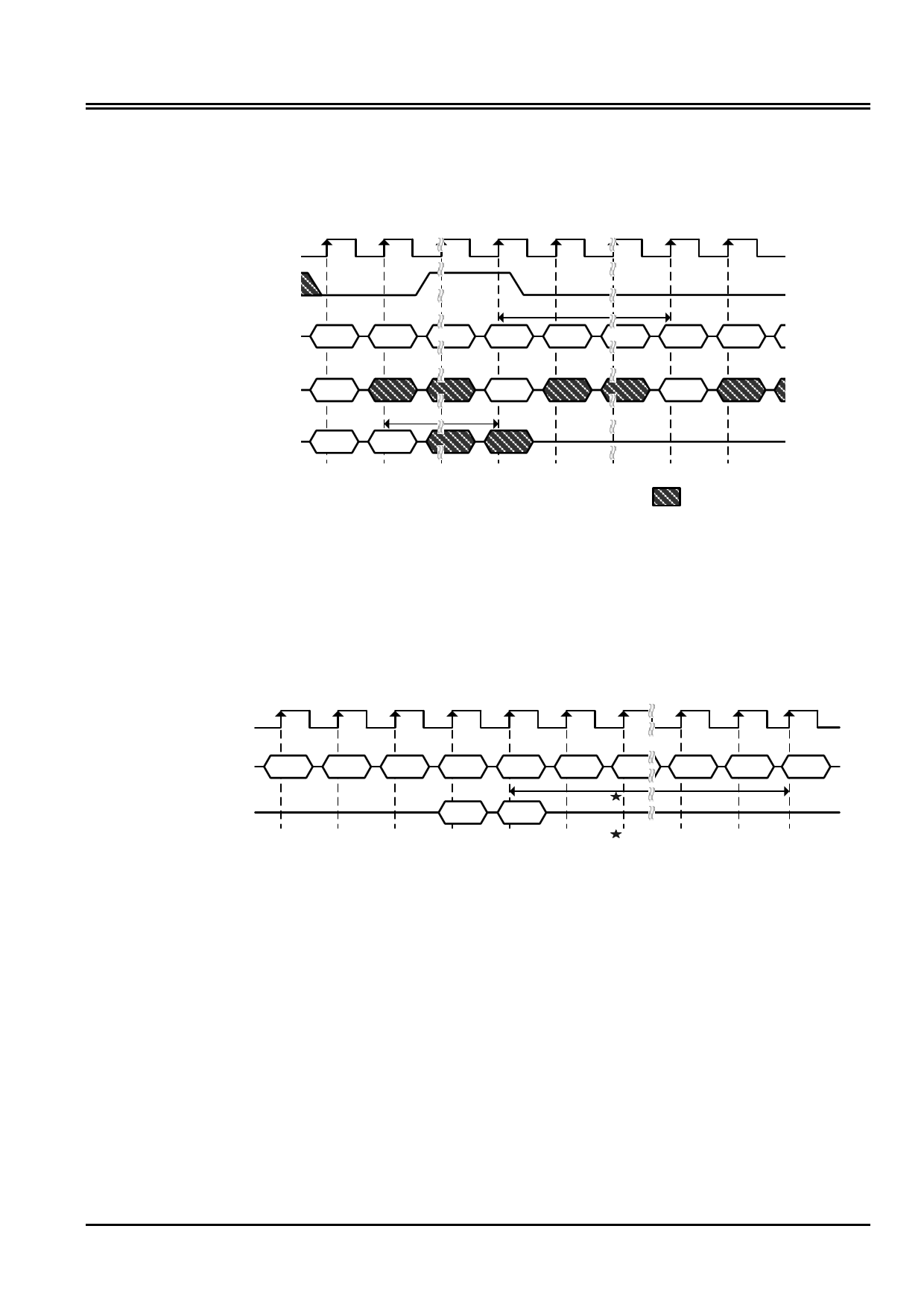
The BankPrecharge/PrechargeAll command that interrupts a write burst without the auto precharge function
should be issued m cycles after the clock edge in which the last data-in element is registered, where m equals
tWR/tCK rounded up to the next whole number. In addition, the DQM signals must be used to mask input data,
starting with the clock edge following the last data-in element and ending with the clock edge on which the
BankPrecharge/PrechargeAll command is entered (refer to the following figure).
T0 T1 T2 T3 T4 T5 T6 T7
CLK
DQM
COMMAND
WRITE
NOP
NOP
Precharge
tRP
NOP
NOP
Activate
NOP
ADDRESS
DQ
Bank
Col n
DIN
n
tWR
DIN
N+1
Bank (s)
ROW
Don’t Care
Note: The LDQM/UDQM can remain low in this example if the length of the write burst is 1 or 2.
Figure 14. Write to Precharge
7 Write and AutoPrecharge command
(RAS# = "H", CAS# = "L", WE# = "L", BAs = Bank, A10 = "H", A0-A7 = Column Address)
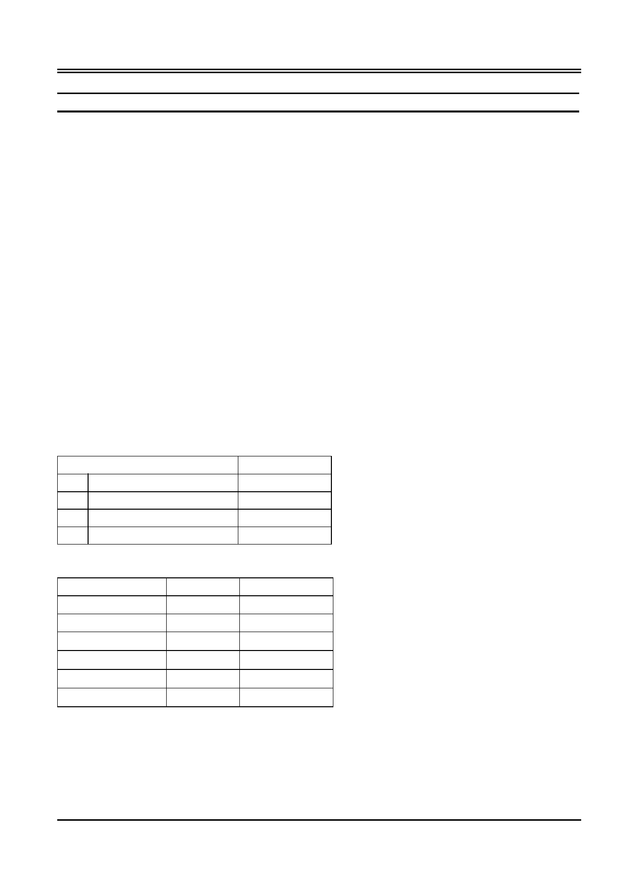
The Write and AutoPrecharge command performs the precharge operation automatically after the write
operation. Once this command is given, any subsequent command can not occur within a time delay of
{(burst length -1) + tWR + tRP(min.)}. At full-page burst, only the write operation is performed in this
command and the auto precharge function is ignored.
T0 T1 T2 T3 T4 T5 T6 T7 T8 T9
CLK
COMMAND
Bank A
Activate
NOP
NOP
WRITE A
Auto Precharge
NOP
NOP
tDAL
NOP
NOP
NOP
DQ
DIN A0
DIN A1
tDAL=tWR+tRP
Begin AutoPrecharge
Bank can be reactivated at
completion of tDAL
Figure 15. Burst Write with Auto-Precharge (Burst Length = 2)
Bank A
Activate
8 Mode Register Set command (RAS# = "L", CAS# = "L", WE# = "L", A0-A11 = Register Data)
The mode register stores the data for controlling the various operating modes of SDRAM. The Mode
Register Set command programs the values of CAS latency, Addressing Mode and Burst Length in the
Mode register to make SDRAM useful for a variety of different applications. The default values of the
Mode Register after power-up are undefined; therefore this command must be issued at the power-up
sequence. The state of pins A0~A9 and A11 in the same cycle is the data written to the mode register.
Two clock cycles are required to complete the write in the mode register (refer to the following figure).
The contents of the mode register can be changed using the same command and the clock cycle
requirements during operation as long as all banks are in the idle state.
Rev. 5.3
11
Dec. /2013
11 Page | ||
| Páginas | Total 30 Páginas | |
| PDF Descargar | [ Datasheet EM638165.PDF ] | |
Hoja de datos destacado
| Número de pieza | Descripción | Fabricantes |
| EM638165 | 4M x 16 bit Synchronous DRAM | Etron Technology |
| EM638165TS | 4M x 16 bit Synchronous DRAM | Etron Technology |
| Número de pieza | Descripción | Fabricantes |
| SLA6805M | High Voltage 3 phase Motor Driver IC. |
Sanken |
| SDC1742 | 12- and 14-Bit Hybrid Synchro / Resolver-to-Digital Converters. |
Analog Devices |
|
DataSheet.es es una pagina web que funciona como un repositorio de manuales o hoja de datos de muchos de los productos más populares, |
| DataSheet.es | 2020 | Privacy Policy | Contacto | Buscar |
