|
|
|
PDF DG412LE Data sheet ( Hoja de datos )
| Número de pieza | DG412LE | |
| Descripción | Quad SPST Switches | |
| Fabricantes | Vishay | |
| Logotipo | ||
Hay una vista previa y un enlace de descarga de DG412LE (archivo pdf) en la parte inferior de esta página. Total 17 Páginas | ||
|
No Preview Available !
www.vishay.com
DG411LE, DG412LE, DG413LE
Vishay Siliconix
16 , Low Parasitic Capacitance and Leakage,
+12 V / +5 V / +3 V / ± 5 V Quad SPST Switches
DESCRIPTION
The DG411LE, DG412LE, and DG413LE are monolithic
quad single-pole-single-throw analog switches. The
DG411LE and DG412LE differ only in that they respond to
opposite logic levels. The DG413LE has two normally open
and two normally closed switches. It can be given various
configurations, including four SPST, two SPDT, and one
DPDT.
The DG411LE, DG412LE, and DG413LE offer low on
resistance of 16 , low parasitic capacitance of 15 pF
switch on capacitance, and low charge injection over the
signal swing range.
The DG411LE, DG412LE, and DG413LE operate on single
and dual supplies. Single supply voltage ranges from 3 V
to 16 V while dual supply operation is recommended with
± 3 V to ± 8 V. Each switch conducts equally well in both
direction when on, and blocks input voltages up to the
supply levels when off.
The DG411LE, DG412LE, and DG413LE are available in
16 lead TSSOP, SOIC, and PDIP packages.
FEATURES
• 3 V to 16 V single supply or ± 3 V to ± 8 V dual
supply
• On-resistance RDS(on): 16
Available
• Low parasitic capacitance:
Available
CD(ON): 15 pF
CS(OFF): 5 pF
• Less than 8 pC charge injection over the full signal swing
range
• Fast switching tON: 16 ns
tOFF: 9 ns
• TTL, CMOS compatible
• Material categorization: for definitions of compliance
please see www.vishay.com/doc?99912
Note
* This datasheet provides information about parts that are
RoHS-compliant and / or parts that are non-RoHS-compliant. For
example, parts with lead (Pb) terminations are not RoHS-compliant.
Please see the information / tables in this datasheet for details.
BENEFITS
• Wide operation voltage range
• Low signal errors and distortion
• Fast switching time
• Minimized switching glitch
APPLICATIONS
• Automatic test equipment
• Data acquisition systems
• Meters and instruments
• Medical and healthcare systems
• Communication systems
• Audio and video signal routing
• Relay replacement
• Battery powered systems
• Computer peripherals
• Audio and video signal routing
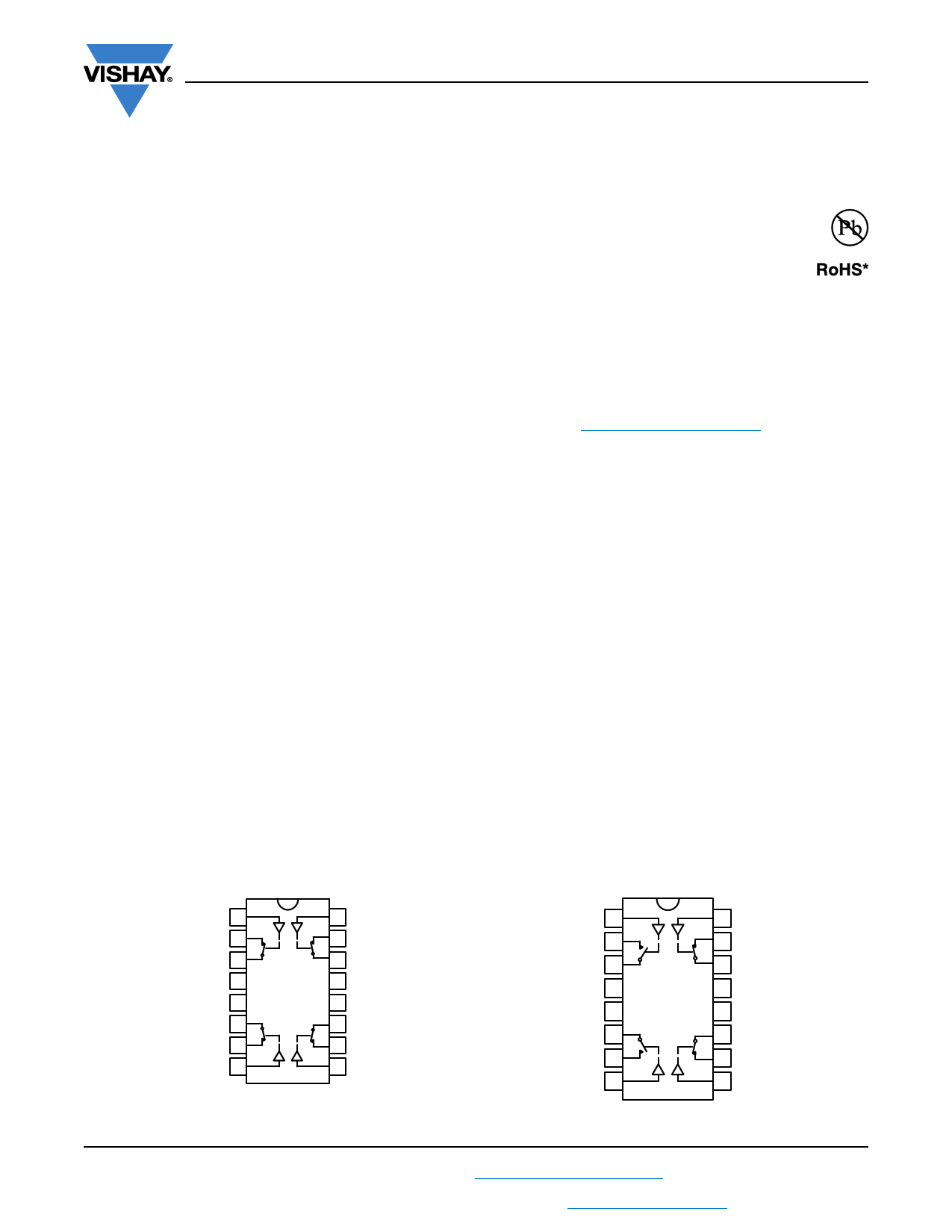
FUNCTIONAL BLOCK DIAGRAM AND PIN CONFIGURATION
DG411LE, DG412LE
Dual-In-Line, TSSOP and SOIC
DG413LE
Dual-In-Line, TSSOP and SOIC
IN1 1
D1 2
S1 3
V- 4
GND 5
S4 6
D4 7
IN4 8
Top View
16 IN2
15 D2
14 S2
13 V+
12 VL
11 S3
10 D3
9 IN3
IN1 1
D1 2
S1 3
V- 4
GND 5
S4 6
D4 7
IN4 8
Top View
16 IN2
15 D2
14 S2
13 V+
12 VL
11 S3
10 D3
9 IN3
S16-0391-Rev. A, 07-Mar-16
1
Document Number: 78091
For technical questions, contact: [email protected]
THIS DOCUMENT IS SUBJECT TO CHANGE WITHOUT NOTICE. THE PRODUCTS DESCRIBED HEREIN AND THIS DOCUMENT
ARE SUBJECT TO SPECIFIC DISCLAIMERS, SET FORTH AT www.vishay.com/doc?91000
1 page 
www.vishay.com
DG411LE, DG412LE, DG413LE
Vishay Siliconix
SPECIFICATIONS a (Single Supply 5 V)
PARAMETER
SYMBOL
Analog Switch
Analog Signal Range e
Drain-Source
On-Resistance e
Dynamic Characteristics
VANALOG
RDS(on)
TEST CONDITIONS
UNLESS OTHERWISE
SPECIFIED
V+ = 5 V, V- = 0 V
VL = 5 V, VIN = 2.4 V, 0.8 V f
V+ = 4.5 V,
IS = 5 mA, VD = 1 V, 3.5 V
A SUFFIX
D SUFFIX
LIMITS
LIMITS
TEMP.b TYP. c -55 °C to +125 °C -40 °C to +85 °C UNIT
MIN. d MAX. d MIN. d MAX. d
Full - - 5 - 5 V
Room 36 - 50 - 50
Full -
- 88 - 75
Turn-On Time e
Turn-Off Time e
Room 27 - 50 - 50
tON
RL = 300 , CL = 35 pF,
Hot -
- 90 - 60
tOFF
VS = 3.5 V, see figure 2 Room 15 - 30 - 30 ns
Hot -
- 55 - 40
Break-Before-Make Time
Delay e
tD
DG413L only, VS = 3.5 V,
RL = 300 , CL = 35 pF
Room 11
-
-
-
-
Charge Injection e
Q Vg = 0 V, Rg = 0 , CL = 10 nF Room 3.3 - - - - pC
Power Supplies
Positive Supply Current e
I+
Room 0.02
-
1
-
Hot -
- 7.5 -
1
5
Negative Supply Current e
Logic Supply Current e
I-
IL
VIN = 0 V or 5 V
Room -0.002 -1 - -1 -
Hot - -7.5 - -5 -
μA
Room 0.002
-
1
-
1
Hot -
- 7.5 -
5
Ground Current e
IGND
Room -0.002 -1 - -1 -
Hot - -7.5 - -5 -
Notes
a. Refer to PROCESS OPTION FLOWCHART.
b. Room = 25 °C, full = as determined by the operating temperature suffix.
c. Typical values are for DESIGN AID ONLY, not guaranteed nor subject to production testing.
d. The algebraic convention whereby the most negative value is a minimum and the most positive a maximum, is used in this datasheet.
e. Guaranteed by design, not subject to production test.
f. VIN = input voltage to perform proper function.
g. Leakage parameters are guaranteed by worst case test conditions and not subject to test.
S16-0391-Rev. A, 07-Mar-16
5
Document Number: 78091
For technical questions, contact: [email protected]
THIS DOCUMENT IS SUBJECT TO CHANGE WITHOUT NOTICE. THE PRODUCTS DESCRIBED HEREIN AND THIS DOCUMENT
ARE SUBJECT TO SPECIFIC DISCLAIMERS, SET FORTH AT www.vishay.com/doc?91000
5 Page 
www.vishay.com
TEST CIRCUITS
DG411LE, DG412LE, DG413LE
Vishay Siliconix
VL
C
V+
C
VS
Rg = 50 Ω
0 V, 2.4 V
NC
VL
S1
IN1
S2
0 V, 2.4 V
IN2
GND
XTALK Isolation = 20 log
C = RF bypass
VS
VO
Fig. 5 - Crosstalk
V+
D1
D2
V- C
V-
50 Ω
VO
RL
VL
C
VS
Rg = 50 Ω
0 V, 2.4 V
VL
S
IN
GND
V+
V+
D
C
VO
V- C
RL
50 Ω
VL
C
VL
IN
0 V, 2.4 V
V+
C
V+
S
D
Meter
HP4192A
Impedance
Analyzer
or Equivalent
V-
GND
V-
C
Off Isolation = 20 log
C = RF Bypass
VS
VO
V-
Fig. 6 - Off-Isolation
Fig. 7 - Source / Drain Capacitances
Vishay Siliconix maintains worldwide manufacturing capability. Products may be manufactured at one of several qualified locations. Reliability data for Silicon
Technology and Package Reliability represent a composite of all qualified locations. For related documents such as package/tape drawings, part marking, and
reliability data, see www.vishay.com/ppg?78091.
S16-0391-Rev. A, 07-Mar-16
11
Document Number: 78091
For technical questions, contact: [email protected]
THIS DOCUMENT IS SUBJECT TO CHANGE WITHOUT NOTICE. THE PRODUCTS DESCRIBED HEREIN AND THIS DOCUMENT
ARE SUBJECT TO SPECIFIC DISCLAIMERS, SET FORTH AT www.vishay.com/doc?91000
11 Page | ||
| Páginas | Total 17 Páginas | |
| PDF Descargar | [ Datasheet DG412LE.PDF ] | |
Hoja de datos destacado
| Número de pieza | Descripción | Fabricantes |
| DG412L | Precision Monolithic Quad SPST Low-Voltage CMOS Analog Switches | Vishay |
| DG412LE | Quad SPST Switches | Vishay |
| Número de pieza | Descripción | Fabricantes |
| SLA6805M | High Voltage 3 phase Motor Driver IC. |
Sanken |
| SDC1742 | 12- and 14-Bit Hybrid Synchro / Resolver-to-Digital Converters. |
Analog Devices |
|
DataSheet.es es una pagina web que funciona como un repositorio de manuales o hoja de datos de muchos de los productos más populares, |
| DataSheet.es | 2020 | Privacy Policy | Contacto | Buscar |