|
|
|
PDF 9ZX21201 Data sheet ( Hoja de datos )
| Número de pieza | 9ZX21201 | |
| Descripción | 12-OUTPUT DIFFERENTIAL Z-BUFFER | |
| Fabricantes | IDT | |
| Logotipo | ||
Hay una vista previa y un enlace de descarga de 9ZX21201 (archivo pdf) en la parte inferior de esta página. Total 16 Páginas | ||
|
No Preview Available !
DATASHEET
12-OUTPUT DIFFERENTIAL Z-BUFFER FOR PCIE GEN2/3 AND QPI 9ZX21201
General Description
The IDT9ZX21201 is a 12-output DB1200Z suitable for PCI-Express
Gen3 or QPI applications. The part is backwards compatible to
PCIe Gen1 and Gen2. A fixed external feedback maintains low drift
for critical QPI applications. In bypass mode, the IDT9ZX21201 can
provide outputs up to 150MHz.
Recommended Application
12-output PCIe Gen3/ QPI differential buffer for Romley and newer
platforms
Key Specifications
• Cycle-to-cycle jitter <50ps
• Output-to-output skew < 65 ps
• Input-to-output delay variation <50ps
• PCIe Gen3 phase jitter < 1.0ps RMS
• QPI 9.6GT/s 12UI phase jitter < 0.2ps RMS
Features/Benefits
• Space-saving 64-pin packages
• Fixed feedback path/ 0ps input-to-output delay
• 9 Selectable SMBus Addresses/Mulitple devices can share
the same SMBus Segment
• 12 OE# pins/Hardware control of each output
• PLL or bypass mode/PLL can dejitter incoming clock
• 100MHz or 133MHz PLL mode operation/supports PCIe
and QPI applications
• Selectable PLL bandwidth/minimizes jitter peaking in
downstream PLL's
• Spread Spectrum Compatible/tracks spreading input clock
for low EMI
• Software control of PLL Bandwidth and Bypass Settings/
PLL can dejitter incoming clock (B Rev only)
Output Features
• 12 - 0.7V differential HCSL output pairs
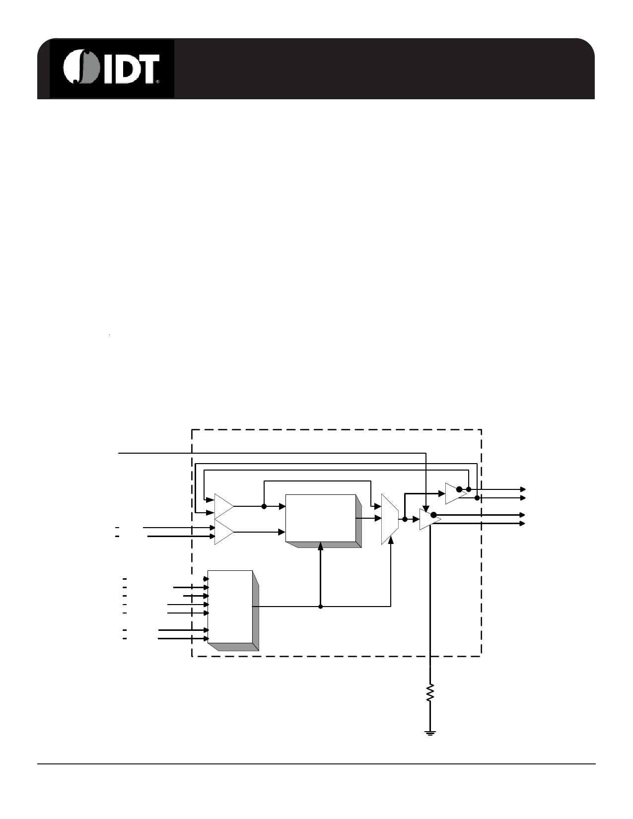
Functional Block Diagram
OE(11:0)#
DIF_IN
DIF_IN#
HIBW_BYPM_LOBW#
100M_133M#
CKPWRGD/PD#
SMB_A0_tri
SMB_A1_tri
SMBDAT
SMBCLK
Logic
Z-PLL
(SS Compatible)
DFB_OUT
DIF(11:0)
Note: Even though the feedback is fixed, DFB_OUT still needs a
termination network for the part to function.
IDT® 12-Output Differential Z-buffer for PCIe Gen2/3 and QPI
1
IREF
1682D - 11/19/15
1 page 
9ZX21201
12-Output Differential Z-buffer for PCIe Gen2/3 and QPI
Electrical Characteristics - Absolute Maximum Ratings
PARAMETER
SYMBOL
CONDITIONS
3.3V Core Supply Voltage VDD, VDDA
VDD for core logic and PLL
Input Low Voltage
VIL
Input High Voltage
VIH
Except for SMBus interface
Input High Voltage
VIHSMB
SMBus clock and data pins
Storage Temperature
Ts
Junction Temperature
Tj
Input ESD protection
ESD prot
Human Body Model
1Guaranteed by design and characterization, not 100% tested in production.
2 Operation under these conditions is neither implied nor guaranteed.
Electrical Characteristics - Input/Supply/Common Parameters
MIN
GND-0.5
-65
2000
TYP
UNITS NOTES
MAX
4.6 V 1,2
V1
VDD+0.5V
5.5V
V
V
1
1
150 °C 1
125 °C 1
V1
TA = TCOM; Supply Voltage VDD/VDDA = 3.3 V +/-5%
PARAMETER
SYMBOL
CONDITIONS
MIN TYP MAX UNITS NOTES
Ambient Operating
Temperature
Input High Voltage
Input Low Voltage
TCOM
VIH
VIL
IIN
Commmercial range
Single-ended inputs, except SMBus, low
threshold and tri-level inputs
Single-ended inputs, except SMBus, low
threshold and tri-level inputs
Single-ended inputs, VIN = GND, VIN = VDD
0
2
GND - 0.3
-5
70 °C
VDD + 0.3 V
0.8 V
5 uA
1
1
1
1
Input Current
Single-ended inputs
IINP
VIN = 0 V; Inputs with internal pull-up resistors
-200
VIN = VDD; Inputs with internal pull-down resistors
200 uA 1
Input Frequency
Pin Inductance
Capacitance
Fibyp
Fipll
Fipll
Lpin
CIN
CINDIF_IN
VDD = 3.3 V, Bypass mode
VDD = 3.3 V, 100MHz PLL mode
VDD = 3.3 V, 133.33MHz PLL mode
Logic Inputs, except DIF_IN
DIF_IN differential clock inputs
33 150
90 100.00 110
120 133.33 147
7
1.5 5
1.5 2.7
MHz
MHz
MHz
nH
pF
pF
2
2
2
1
1
1,4
COUT
Output pin capacitance
6 pF 1
Clk Stabilization
TSTAB
From VDD Power-Up and after input clock
stabilization or de-assertion of PD# to 1st clock
0.300
1
ms 1,2
Input SS Modulation
Frequency
fMODIN
Allowable Frequency
(Triangular Modulation)
30
33 kHz 1
OE# Latency
tLATOE#
DIF start after OE# assertion
DIF stop after OE# deassertion
4 6 12 clocks 1
Tdrive_PD#
tDRVPD
DIF output enable after
PD# de-assertion
16 300 us 1,3
Tfall
Trise
SMBus Input Low Voltage
SMBus Input High Voltage
SMBus Output Low Voltage
SMBus Sink Current
Nominal Bus Voltage
SCLK/SDATA Rise Time
SCLK/SDATA Fall Time
SMBus Operating
Frequency
tF
tR
VILSMB
VIHSMB
VOLSMB
IPULLUP
VDDSMB
tRSMB
tFSMB
fMAXSMB
Fall time of control inputs
Rise time of control inputs
@ IPULLUP
@ VOL
3V to 5V +/- 10%
(Max VIL - 0.15) to (Min VIH + 0.15)
(Min VIH + 0.15) to (Max VIL - 0.15)
Maximum SMBus operating frequency
2.1
4
2.7
10
10
0.8
VDDSMB
0.4
5.5
1000
300
100
ns
ns
V
V
V
mA
V
ns
ns
kHz
1,2
1,2
1
1
1
1
1
1
1
1,5
1Guaranteed by design and characterization, not 100% tested in production.
2Control input must be monotonic from 20% to 80% of input swing.
3Time from deassertion until outputs are >200 mV
4DIF_IN input
5The differential input clock must be running for the SMBus to be active
IDT® 12-Output Differential Z-buffer for PCIe Gen2/3 and QPI
1682D- 11/19/15
5
5 Page 
9ZX21201
12-Output Differential Z-buffer for PCIe Gen2/3 and QPI
SMBusTable: PLL Mode, and Frequency Select Register
Byte 0 Pin #
Name
Control Function
Bit 7
5
PLL Mode 1
PLL Operating Mode Rd back 1
Bit 6
5
PLL Mode 0
PLL Operating Mode Rd back 0
Bit 5
Reserved
Bit 4
Reserved
Bit 3 These bits
PLL_SW_EN
Enable S/W control of PLL BW
Bit 2 available in B
PLL Mode 1
PLL Operating Mode 1
Bit 1 rev only.
PLL Mode 0
PLL Operating Mode 1
Bit 0
4
100M_133M#
Frequency Select Readback
SMBusTable: Output Control Register
Byte 1 Pin #
Name
Bit 7
47/46
DIF_7_En
Bit 6
43/42
DIF_6_En
Bit 5
39/38
DIF_5_En
Bit 4
35/34
DIF_4_En
Bit 3
30/31
DIF_3_En
Bit 2
26/27
DIF_2_En
Bit 1
21/22
DIF_1_En
Bit 0
17/18
DIF_0_En
Control Function
Output Control - '0' overrides OE# pin
Output Control - '0' overrides OE# pin
Output Control - '0' overrides OE# pin
Output Control - '0' overrides OE# pin
Output Control - '0' overrides OE# pin
Output Control - '0' overrides OE# pin
Output Control - '0' overrides OE# pin
Output Control - '0' overrides OE# pin
SMBusTable: Output Control Register
Byte 2 Pin #
Name
Bit 7
Bit 6
Bit 5
Bit 4
Bit 3
64/63
DIF_11_En
Bit 2
59/60
DIF_10_En
Bit 1
54/55
DIF_9_En
Bit 0
50/51
DIF_8_En
Control Function
Reserved
Reserved
Reserved
Reserved
Output Control - '0' overrides OE# pin
Output Control - '0' overrides OE# pin
Output Control - '0' overrides OE# pin
Output Control - '0' overrides OE# pin
SMBusTable: Reserved Register
Byte 3 Pin #
Name
Bit 7
Bit 6
Bit 5
Bit 4
Bit 3
Bit 2
Bit 1
Bit 0
Control Function
Reserved
Reserved
Reserved
Reserved
Reserved
Reserved
Reserved
Reserved
Type
R
R
RW
RW
RW
R
Type
RW
RW
RW
RW
RW
RW
RW
RW
Type
RW
RW
RW
RW
Type
01
See PLL Operating Mode
Readback Table
HW Latch S/W Control
See PLL Operating Mode
Readback Table
133MHz
100MHz
Default
Latch
Latch
0
0
0
1
1
Latch
0
Low/Low
1
Enable
Default
1
1
1
1
1
1
1
1
0
Low/Low
1
Enable
Default
0
0
0
0
1
1
1
1
0 1 Default
0
0
0
0
0
0
0
0
IDT® 12-Output Differential Z-buffer for PCIe Gen2/3 and QPI
11
1682D- 11/19/15
11 Page | ||
| Páginas | Total 16 Páginas | |
| PDF Descargar | [ Datasheet 9ZX21201.PDF ] | |
Hoja de datos destacado
| Número de pieza | Descripción | Fabricantes |
| 9ZX21200 | 12-OUTPUT DIFFERENTIAL Z-BUFFER | IDT |
| 9ZX21201 | 12-OUTPUT DIFFERENTIAL Z-BUFFER | IDT |
| Número de pieza | Descripción | Fabricantes |
| SLA6805M | High Voltage 3 phase Motor Driver IC. |
Sanken |
| SDC1742 | 12- and 14-Bit Hybrid Synchro / Resolver-to-Digital Converters. |
Analog Devices |
|
DataSheet.es es una pagina web que funciona como un repositorio de manuales o hoja de datos de muchos de los productos más populares, |
| DataSheet.es | 2020 | Privacy Policy | Contacto | Buscar |