|
|
|
PDF 831752 Data sheet ( Hoja de datos )
| Número de pieza | 831752 | |
| Descripción | Clock Switch | |
| Fabricantes | IDT | |
| Logotipo | ||
Hay una vista previa y un enlace de descarga de 831752 (archivo pdf) en la parte inferior de esta página. Total 18 Páginas | ||
|
No Preview Available !
Clock Switch for ATCA/AMC and PCIe
Applications
831752
Data Sheet
General Description
The 831752 is a high-performance, differential HCSL clock switch.
The device is designed for the routing of PCIe clock signals in
ATCA/AMC system and is optimized for PCIe Gen 1, Gen 2 and Gen
3. The device has one differential, bi-directional I/O (FCLK) for
connection to ATCA clock sources and to clock receivers through a
connector. The differential clock input CLK is the local clock input
and the HCSL output Q is the local clock output. In the common
clock mode, FCLK serves as an input and is routed to the differential
HCSL output Q. There are two local clock modes. In the local clock
mode 0, CLK is the input, Q is the clock output and FCLK is in
high-impedance state. In the local clock mode 1, CLK is the input
and both Q and FCLK are the outputs of the locally generated PCIe
clock signal. The 831752 is characterized to operate from a 3.3V
power or 2.5V power supply. The 831752 supports the switching of
PCI Express (2.5 Gb/s), Gen 2 (5 Gb/s) and Gen 3 (8 Gb/s) clock
signals.
Pin Assignment
Features
• Clock switch for PCIe and ATCA/AMC applications
• Supports local and common ATCA/AMC clock modes
• Bi-directional clock I/O FCLK:
- When operating as an output, FCLK is a source-terminated
HCSL signal.
- When operating as an input, FCLK accepts HCSL, LVDS and
LVPECL levels.
• Local clock input (CLK) accepts HCSL, LVDS and LVPECL
differential signals
• Local HCSL clock output (Q)
• Maximum input/output clock frequency: 500MHz
• Maximum input/output data rate: 1000Mb/s (NRZ)
• LVCMOS interface levels for the control inputs
• PCI Express (2.5 Gb/S), Gen 2 (5 Gb/s) and Gen 3 (8 Gb/s) jitter
compliant
• Full 3.3V or 2.5V supply voltage
• Lead-free (RoHS 6) 16-lead TSSOP package
• -40°C to 85°C ambient operating temperature
DIR_SEL
nOEFCLK
VDD
FCLK
nFCLK
GND
CLK
nCLK
1
2
3
4
5
6
7
8
16 IREF
15 GND
14 VDD
13 Q
12 nQ
11 GND
10 VDD
9 nc
831752
16-lead TSSOP
4.4mm x 5.0mm x 0.925mm package body
G Package, Top View
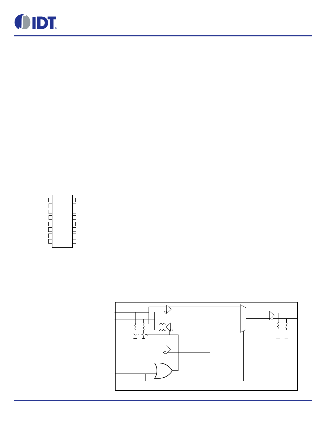
Block Diagram
FCLK
nFCLK
50 50
22.33
22.33
CLK Pulldown
nCLK Pullup/Pulldown
nOEFCLK Pullup
DIR_SEL Pulldown
IREF
1=disable
1Q
nQ
0 50 50
©2016 Integrated Device Technology, Inc
1
Revision B June 28, 2016
1 page 
831752 Data Sheet
Table 5B. HCSL AC Characteristics, VDD = 3.3V±5% or 2.5V±5%, TA = -40°C to 85°C
Symbol
Parameter
Test Conditions
Minimum
fOUT
tjit
Output Frequency
Buffer Additive Phase Jitter, RMS;
refer to Additive Phase Jitter Plot
100MHz, Integration Range:
12kHz – 20MHz
FCLK to Q
1.75
tPD Propagation Delay, NOTE 1
CLK to Q
CLK to FCLK
1.95
1.50
MUXISOL
Edge Rate
Mux Isolation
Rise/Fall Edge Rate; NOTE 2, 3
f = 100MHz
0.6
VRB
tSTABLE
Ringback Voltage; NOTE 2, 4
Time before VRB is allowed;
NOTE 2, 4
-100
500
VMAX
Absolute Max Output Voltage;
NOTE 5, 6
VMIN
Absolute Min Output Voltage;
NOTE 5, 7
-300
VCROSS
Absolute Crossing Voltage;
NOTE 5, 8, 9
250
VCROSS
Total Variation of VCROSS over all
edges; NOTE 5, 8, 10
odc Output Duty Cycle; NOTE 11
f 312.5MHz
f > 312.5MHz
44
40
Typical
100
0.3
-70
800
-35
385
40
50
50
Maximum
500
0.505
3.65
3.90
3.70
4
100
1350
650
140
56
60
Units
MHz
ps
ns
ns
ns
dB
V/ns
mV
ps
mV
mV
mV
mV
%
NOTE: Measurements taken with Q output and FCLK output.
NOTE: Electrical parameters are guaranteed over the specified ambient operating temperature range, which is established when the device is
mounted in a test socket with maintained transverse airflow greater than 500 lfpm. The device will meet specifications after thermal equilibrium
has been reached under these conditions.
NOTE: All measurements were taken with FCLK, nFCLK and Q, nQ operating as outputs unless otherwise noted.
NOTE 1: Measured from the differential input cross point to the differential output crossing point.
NOTE 2: Measurement taken from differential waveform.
NOTE 3: Measurement from -150mV to +150mV on the differential waveform (derived from Q minus nQ). The signal must be monotonic
through the measurement region for rise and fall time. The 300mV measurement window is centered on the differential zero crossing.
NOTE 4: TSTABLE is the time the differential clock must maintain a minimum ±150mV differential voltage after rising/falling edges before it is
allowed to drop back into the VRB ±100 differential range. See Parameter Measurement Information Section.
NOTE 5: Measurement taken from single-ended waveform.
NOTE 6: Defined as the maximum instantaneous voltage including overshoot. See Parameter Measurement Information Section.
NOTE 7: Defined as the minimum instantaneous voltage including undershoot. See Parameter Measurement Information Section.
NOTE 8: Measured at crossing point where the instantaneous voltage value of the rising edge of Q equals the falling edge of nQ.
See Parameter Measurement Information Section.
NOTE 9: Refers to the total variation from the lowest crossing point to the highest, regardless of which edge is crossing. Refers to all crossing
points for this measurement. See Parameter Measurement Information Section.
NOTE 10: Defined as the total variation of all crossing voltage of rising Q and falling nQ. This is the maximum allowed variance in the VCROSS
for any particular system. See Parameter Measurement Information Section.
NOTE 11: Input duty cycle must be 50%.
NOTE 12: Matching applies to rising edge rate for Q and falling edge rate for nQ. It is measured using a ±75mV window centered on the
median crosspoint where Q meets nQ falling. The median crosspoint is used to calculate the voltage thresholds the oscilloscope is to use for
the edge rate calculations. The rise edge rate of Q should be compared to the fall edge rate of nQ, the maximum allowed difference should not
exceed 20% of the slowest edge rate.
©2016 Integrated Device Technology, Inc
5
Revision B June 28, 2016
5 Page 
831752 Data Sheet
2.5V Differential Clock Input Interface
The CLK/nCLK accepts HCSL, LVDS and LVPECL and other
differential signals. Both differential signals must meet the VPP and
VCMR input requirements. Figures 4A to 4 E show interface examples
for the CLK/nCLK input driven by the most common driver types. The
input interfaces suggested here are examples only. If the driver is
from another vendor, use their termination recommendation. Please
consult with the vendor of the driver component to confirm the driver
termination requirements. The figures below also apply to FCLK/
nFCLK operating as an input.
2.5V
2.5V
*R3 33
Zo = 50
Zo = 50
HCSL
*R4 33
*Optional – R3 and R4 can be 0
R1
50
CLK
nCLK
R2
50
Differential
Input
Figure 4A. CLK/nCLK Input Driven by a 2.5V LVPECL
Driver
Figure 4B. CLK/nCLK Input Driven by a 2.5V HCSL Driver
2.5V
2.5V LVPECL
Zo = 50Ω
Zo = 50Ω
R5
100 - 200
R6
100 - 200
2.5V
R3
84
C1
R4
84
C2
R1 R2
125 125
2.5V
CLK
nCLK
Differential
Input
Figure 4C. CLK/nCLK Input Driven by a 2.5V LVPECL
Driver
Figure 4D. CLK/nCLK Input Driven by a 2.5V LVPECL
Driver with AC Couple
Figure 4E. CLK/nCLK Input Driven by a 2.5V LVDS Driver
©2016 Integrated Device Technology, Inc
11
Revision B June 28, 2016
11 Page | ||
| Páginas | Total 18 Páginas | |
| PDF Descargar | [ Datasheet 831752.PDF ] | |
Hoja de datos destacado
| Número de pieza | Descripción | Fabricantes |
| 831752 | Clock Switch | IDT |
| Número de pieza | Descripción | Fabricantes |
| SLA6805M | High Voltage 3 phase Motor Driver IC. |
Sanken |
| SDC1742 | 12- and 14-Bit Hybrid Synchro / Resolver-to-Digital Converters. |
Analog Devices |
|
DataSheet.es es una pagina web que funciona como un repositorio de manuales o hoja de datos de muchos de los productos más populares, |
| DataSheet.es | 2020 | Privacy Policy | Contacto | Buscar |