|
|
|
PDF LD39100 Data sheet ( Hoja de datos )
| Número de pieza | LD39100 | |
| Descripción | low-noise voltage regulator | |
| Fabricantes | STMicroelectronics | |
| Logotipo | ||
Hay una vista previa y un enlace de descarga de LD39100 (archivo pdf) en la parte inferior de esta página. Total 27 Páginas | ||
|
No Preview Available !
LD39100
1 A, low quiescent current, low-noise voltage regulator
Datasheet - production data
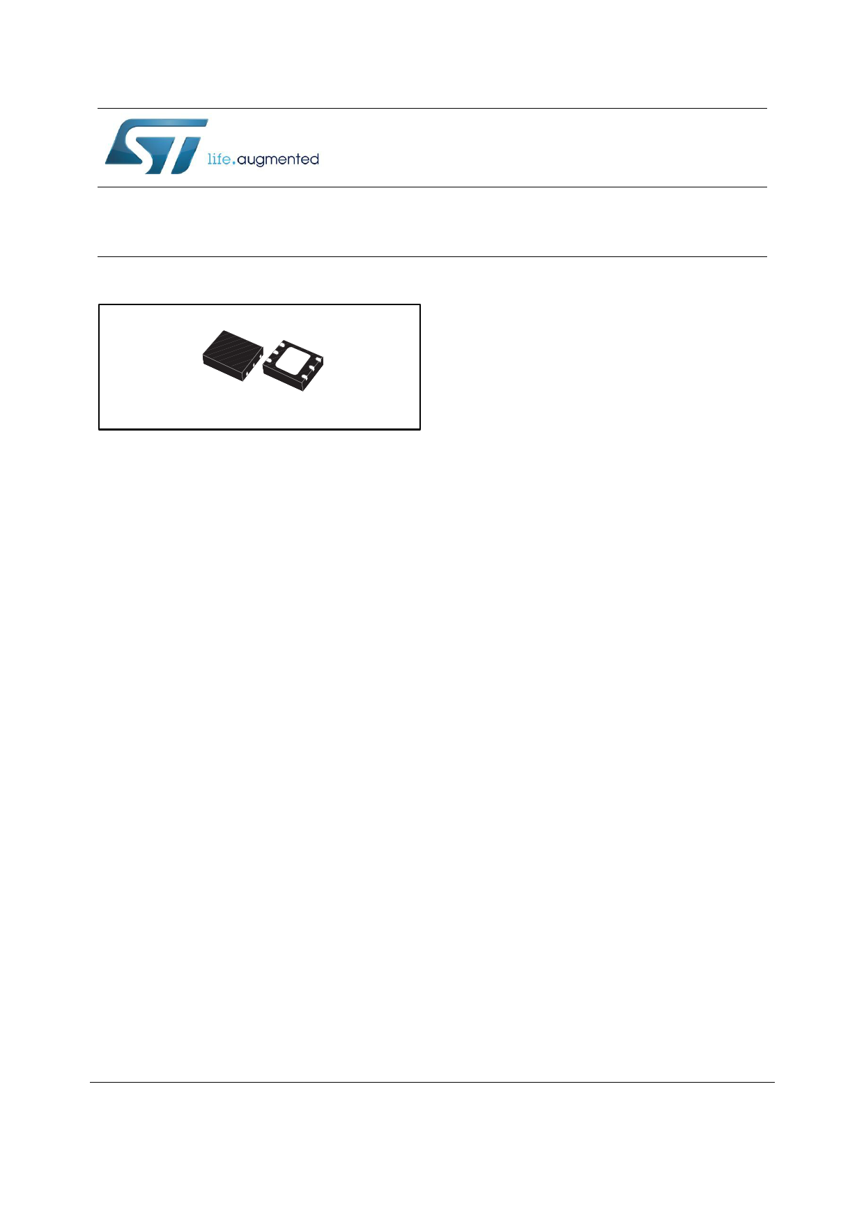
DFN6 (3x3 mm)
Features
Industrial & Automotive grade (AEC-Q100)
Input voltage from 1.5 to 5.5 V
Ultra low-dropout voltage (200 mV typ. at
1 A load)
Very low quiescent current (20 µA typ. at no
load, 200 µA typ. at 1 A load, 1 µA max. in
off mode)
Very low-noise with no bypass capacitor
(30 µ VRMS at VOUT = 0.8 V)
Output voltage tolerance: ± 2.0% @ 25 °C
1 A guaranteed output current
Wide range of output voltages available on
request: 0.8 V to 4.5 V with 100 mV step and
adjustable from 0.8 V
Logic-controlled electronic shutdown
Stable with ceramic capacitors COUT = 1 µF
Internal current and thermal limit
DFN6 (3x3 mm) package
Temperature range: - 40 °C to 125 °C
Applications
Printers
Game consoles
Computer
Consumer applications
Automotive post regulation
Description
The LD39100 provides 1 A maximum current with
an input voltage range from 1.5 V to 5.5 V and a
typical dropout voltage of 200 mV. The device is
stable with ceramic capacitors on the input and
output. The ultra low drop voltage, low quiescent
current and low-noise features make it suitable
for low power battery-powered applications.
Power supply rejection is 70 dB at low frequency
and starts to roll off at 10 kHz. Enable logic
control function puts the LD39100 in shutdown
mode, allowing a total current consumption lower
than 1 µA. The device also includes short-circuit
constant current limiting and thermal protection.
LD39100 is available also in AEC-Q100 qualified
version, in the DFN6 (3x3 mm) with wettable
flank package.
June 2016
DocID15676 Rev 6
This is information on a product in full production.
1/27
www.st.com
1 page 
LD39100
Maximum ratings
3 Maximum ratings
Symbol
Table 2: Absolute maximum ratings
Parameter
Value
Unit
VIN
VOUT
EN
PG
ADJ
IOUT
PD
TSTG
TOP
DC input voltage
DC output voltage
Enable pin
Power Good pin
Adjust pin
Output current
Power dissipation
Storage temperature range
Operating junction temperature range
-0.3 to 7
-0.3 to VIN + 0.3
(7 V max.)
-0.3 to VIN + 0.3
(7 V max.)
-0.3 to 7
4
Internally limited
Internally limited
- 65 to 150
- 40 to 125
V
V
V
V
V
°C
°C
Absolute maximum ratings are those values beyond which damage to the device
may occur. Functional operation under these conditions is not implied. All values
are referred to GND.
Symbol
RthJA
RthJC
Table 3: Thermal data
Parameter
Thermal resistance junction-ambient
Thermal resistance junction-case
Value
55
10
Unit
°C/W
°C/W
Symbol
ESD
Table 4: ESD performance
Parameter
Test conditions
ESD protection voltage
HBM
MM
Value
4
0.4
Unit
kV
kV
DocID15676 Rev 6
5/27
5 Page 
LD39100
Figure 10: Output voltage vs. input voltage
(VOUT = 0.8 V)
1.2
VIN from 0 to 5.5 V, VEN to VIN, VOUT = 0.8 V, IOUT = 1 A
1
0.8
125°C
0.6 85°C
55°C
0.4 25°C
0°C
0.2 -25°C
-40°C
0
0 0.5 1 1.5 2 2.5 3 3.5 4 4.5 5 5.5 6
VIN [V]
GIPD020920151106MT
Typical performance characteristics
Figure 11: Output voltage vs. input voltage
(VOUT = 2.5 V)
3
VIN from 0 to 5V, VEN to VIN, VOUT = 2.5 V, IOUT = 1A
2.5
2 125°C
85°C
1.5 55°C
25°C
1 0°C
0.5 -25°C
-40°C
0
0 0.5 1 1.5 2 2.5 3 3.5 4 4.5 5 5.5 6
VIN [V]
GIPD020920151107MT
Figure 12: Quiescent current vs. temperature
140
120
100
80
60
40 VIN = 1.8 V, VEN to VIN, VOUT = 2.5 V
20
0
-50 -25 0
25 50
T [°C]
No Load
IOUT = 1 A
75 100 125 150
GIPD020920151108MT
Figure 13: VIN input current in off mode vs.
temperature
0.6
VIN = 3.5 V, VEN to G ND, VOUT = 2.5 V
0.5
0.4
0.3
0.2
0.1
0
-50 -25
0
25 50 75
T [°C]
100 125 150
GIPD020920151109MT
0.015
0.01
0.005
0
-0.005
-0.01
-0.015
-50
Figure 14: Load regulation
VIN = 3.5 V, IOUT = from 10 mA to 1 A, VEN=VIN, VOUT = 2.5 V
-25 0 25 50 75 100 125 150
T [°C]
GIPD020920151110MT
Figure 15: Line regulation VOUT = 0.8 V
0.04
0.03
V IN = from 1.8 V to 5.5 V , IOUT = 100 m A , V EN = V IN, VOUT = 0.8 V
0.02
0.01
0
-0.01
-0.02
-0.03
-0.04
-50 -25 0 25 50 75 100 125
150
T [°C]
GIPD020920151111MT
DocID15676 Rev 6
11/27
11 Page | ||
| Páginas | Total 27 Páginas | |
| PDF Descargar | [ Datasheet LD39100.PDF ] | |
Hoja de datos destacado
| Número de pieza | Descripción | Fabricantes |
| LD39100 | low-noise voltage regulator | STMicroelectronics |
| LD39100PU12R | Low Noise Voltage Regulator | STMicroelectronics |
| LD39100PU25R | Low Noise Voltage Regulator | STMicroelectronics |
| LD39100PUR | Low Noise Voltage Regulator | ST Microelectronics |
| Número de pieza | Descripción | Fabricantes |
| SLA6805M | High Voltage 3 phase Motor Driver IC. |
Sanken |
| SDC1742 | 12- and 14-Bit Hybrid Synchro / Resolver-to-Digital Converters. |
Analog Devices |
|
DataSheet.es es una pagina web que funciona como un repositorio de manuales o hoja de datos de muchos de los productos más populares, |
| DataSheet.es | 2020 | Privacy Policy | Contacto | Buscar |