|
|
|
PDF HI-2579 Data sheet ( Hoja de datos )
| Número de pieza | HI-2579 | |
| Descripción | 3.3V MIL-STD-1553/1760 Dual Transceiver | |
| Fabricantes | HOLTIC | |
| Logotipo | ||
Hay una vista previa y un enlace de descarga de HI-2579 (archivo pdf) en la parte inferior de esta página. Total 12 Páginas | ||
|
No Preview Available !
July, 2016
HI-2579, HI-2581
3.3V MIL-STD-1553/1760 Dual Transceiver
with Low Profile Integrated Transformers
GENERAL DESCRIPTION
The HI-2579 / HI-2581 are low power CMOS dual
transceivers with integrated transformers designed
to meet the requirements of the MIL-STD-1553 /
MIL-STD-1760 specifications. The dual transceivers
with integrated transformers provide a low profile single
part solution for interfacing a protocol IC or FPGA to a
dual redundant MIL-STD-1553 bus.
The transmitter section of each bus takes complementary
CMOS / TTL Manchester II bi-phase data and converts it
to differential voltages suitable for driving the integrated
isolation transformer. Separate transmitter inhibit control
signals are provided for each transmitter.
The receiver section of the each bus converts the 1553
bus differential data to complementary CMOS / TTL data
suitable for inputting to a Manchester decoder. Each
receiver has a separate enable input which can be used
to force both receiver outputs to logic “0” (HI-2579) or
logic 1 (HI-2581).
The family of parts are available in Industrial -40oC to
+85oC, or Extended, -55oC to +125oC temperature
ranges.
FEATURES
• Dual-redundant MIL-STD-1553 transceivers with
integrated transformers
• Small footprint and low profile package
• Compliant to MIL-STD-1553A and B,
MIL-STD-1760, ARINC 708A
• 3.3V single supply operation
• Less than 1.0W maximum power dissipation
• Industrial and extended temperature ranges
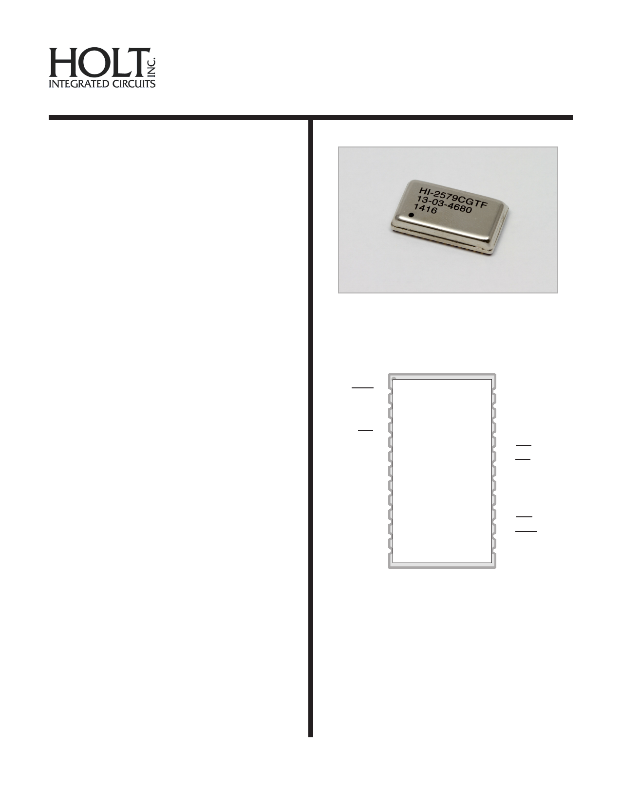
PIN CONFIGURATION (TOP)
BUSA - 1
BUSA - 2
TXA - 3
TXA - 4
VDDA - 5
RXENA - 6
GNDA - 7
VDDB - 8
RXENB - 9
GNDB - 10
DNC - 11
DNC - 12
HI-2579CGIF
HI-2579CGTF
HI-2581CGIF
HI-2581CGTF
24 - DNC
23 - DNC
22 - TXINHA
21 - RXA
20 - RXA
19 - TXB
18 - TXB
17 - TXINHB
16 - RXB
15 - RXB
14 - BUSB
13 - BUSB
DNC = Do Not Connect
DS2579 Rev. E
HOLT INTEGRATED CIRCUITS
www.holtic.com
1
07/16
1 page 
HI-2579, HI-2581
ELECTRICAL CHARACTERISTICS
Table 2. DC Electrical Characteristics
VDD = +3.3V, GND = 0V, TA = Operating Temperature Range (unless otherwise stated)
Parameter
Symbol
Test Conditions
Min Typ Max Units
Operating Voltage
Total Supply Current
VDD
3.15 3.3 3.45
V
ICC1 Not Transmitting
4 17 mA
ICC2 Transmit one bus @ 50% duty cycle
225 320 mA
ICC3
Transmit one bus @ 100% duty
cycle
425 640 mA
Power Dissipation
PD1 Not Transmitting
PD2
Transmit one bus @ 100% duty
cycle
0.06
0.5 1.0
W
W
Min. Input Voltage (HI)
VIH Digital Inputs
Max. Input Voltage (LO)
VIL Digital Inputs
Min. Input Current (HI)
IIH Digital Inputs
Max. Input Current (LO)
IIL Digital Inputs
Min. Output Voltage (HI)
VOH IOUT = -1.0mA, Digital Outputs
Max. Output Voltage (LO)
VOL IOUT = +1.0mA, Digital Outputs
RECEIVER
(Measured at Point “AD” in Figure 4 unless otherwise specified)
2.0
-20
90%
30%
20
10%
V
VDD
μA
μA
VDD
VDD
Input Resistance
Input Capacitance
Common Mode Rejection Ratio
RIN
CIN
CMRR
Differential
Differential
2 kΩ
5 pF
45 dB
Input Common Mode Voltage
Threshold Voltage -
Direct Coupled
Detect
No Detect
Threshold Voltage -
Transformer Coupled
Detect
No Detect
VICM
VTHD
VTHND
VTHD
VTHND
1MHz Sine Wave (measured at
point “AD” in Figure 4)
RXA/B, RXA/B pulse width > 70 ns
No pulse at RXA/B, RXA/B
1MHz Sine Wave (measured at
point “AT” in Figure 5)
RXA/B, RXA/B pulse width > 70 ns
No pulse at RXA/B, RXA/B
-10.0
1.15
0.86
+10.0 V-pk
Vp-p
0.28 Vp-p
Vp-p
0.20 Vp-p
HOLT INTEGRATED CIRCUITS
5
5 Page 
PACKAGE DIMENSIONS
HI-2579, HI-2581
Bottom View
.060
(1.52)
TYP.
24X
.025
(.64)
.660 ± .007
(16.76 ± .18)
.218
(5.54)
Dimensions in inches (mm)
.044
(1.12
SQ.
SQ.)
6X
R.017
(R.43)
Corners
24X
R.008
(R.20)
PIN 1 INDEX
.510 ± .007
(12.95 ± .18)
.600 ± .007
(15.24 ± .18)
Notes:
1. Heatsink pad is internally connected to device GND pins. Connection to external GND for heat extraction is not necessary.
2. The “keep out” zones (crosshatched) enclose test pads for the transformer primary windings. DO NOT CONNECT.
3. Routing traces under the six test pads is not recommended.
HOLT INTEGRATED CIRCUITS
11
11 Page | ||
| Páginas | Total 12 Páginas | |
| PDF Descargar | [ Datasheet HI-2579.PDF ] | |
Hoja de datos destacado
| Número de pieza | Descripción | Fabricantes |
| HI-2579 | 3.3V MIL-STD-1553/1760 Dual Transceiver | HOLTIC |
| Número de pieza | Descripción | Fabricantes |
| SLA6805M | High Voltage 3 phase Motor Driver IC. |
Sanken |
| SDC1742 | 12- and 14-Bit Hybrid Synchro / Resolver-to-Digital Converters. |
Analog Devices |
|
DataSheet.es es una pagina web que funciona como un repositorio de manuales o hoja de datos de muchos de los productos más populares, |
| DataSheet.es | 2020 | Privacy Policy | Contacto | Buscar |