|
|
|
PDF CPV363M4KPbF Data sheet ( Hoja de datos )
| Número de pieza | CPV363M4KPbF | |
| Descripción | IGBT SIP Module | |
| Fabricantes | Vishay | |
| Logotipo | ||
Hay una vista previa y un enlace de descarga de CPV363M4KPbF (archivo pdf) en la parte inferior de esta página. Total 11 Páginas | ||
|
No Preview Available !
www.vishay.com
CPV363M4KPbF
Vishay Semiconductors
IGBT SIP Module
(Short Circuit Rated Ultrafast IGBT)
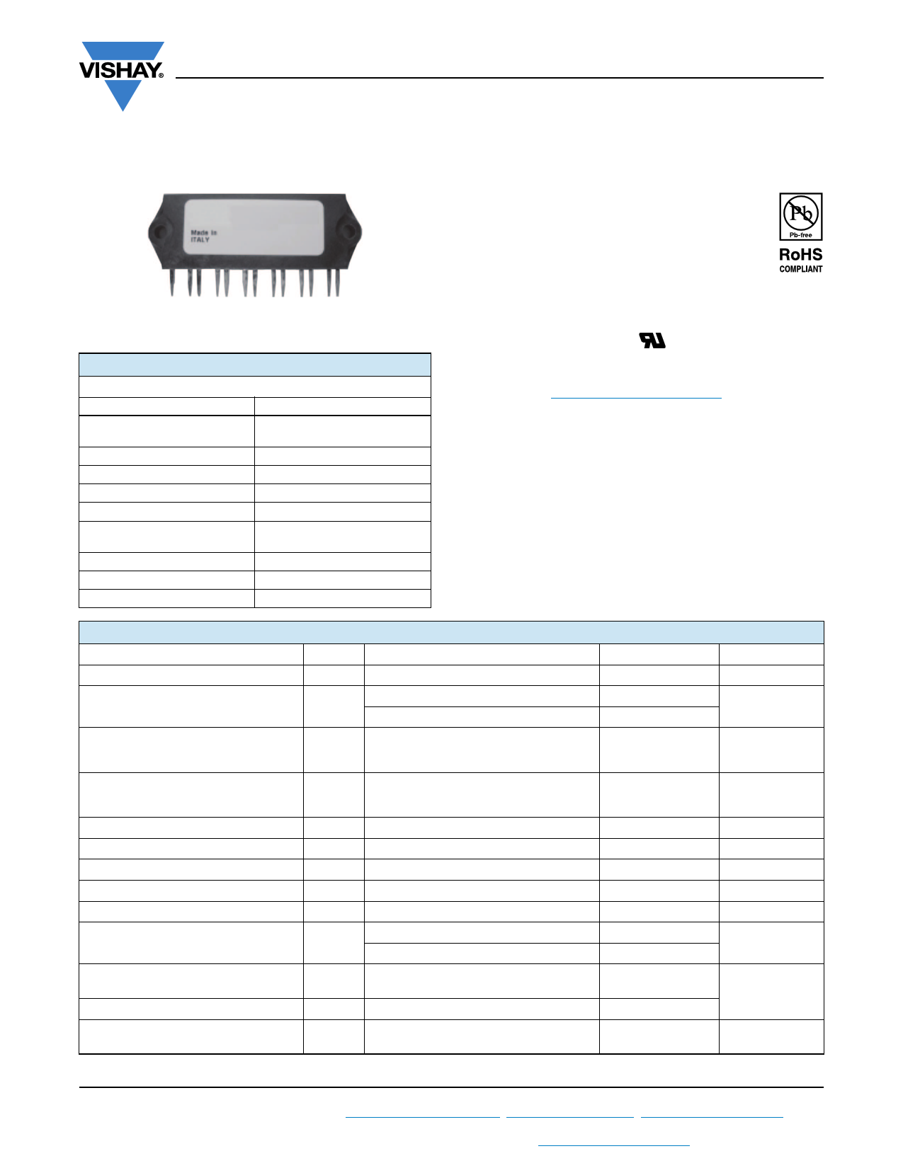
IMS-2
PRODUCT SUMMARY
OUTPUT CURRENT IN A TYPICAL 20 kHz MOTOR DRIVE
VCES
IRMS per phase (1.94 kW total)
with TC = 90 °C
TJ
Supply voltage
Power factor
600 V
6.7 ARMS
125 °C
360 VDC
0.8
Modulation depth (see fig. 1)
VCE(on) (typical)
at IC = 6.0 A, 25 °C
Speed
115 %
1.72 V
8 kHz to 30 kHz
Package
Circuit
SIP
Three phase inverter
FEATURES
• Short circuit rated ultrafast: optimized for high
speed (see fig. 1 for current vs. frequency curve),
and short circuit rated to 10 μs at 125 °C,
VGE = 15 V
• Fully isolated printed circuit board mount
package
• Switching-loss rating includes all “tail” losses
• HEXFRED® soft ultrafast diodes
• UL approved file E78996
• Designed and qualified for industrial level
• Material categorization: for definitions of compliance
please see www.vishay.com/doc?99912
DESCRIPTION
The IGBT technology is the key to Vishay’s Semiconductors
advanced line of IMS (Insulated Metal Substrate) power
modules. These modules are more efficient than
comparable bipolar transistor modules, while at the same
time having the simpler gate-drive requirements of the
familiar power MOSFET. This superior technology has now
been coupled to a state of the art materials system that
maximizes power throughput with low thermal resistance.
This package is highly suited to motor drive applications and
where space is at a premium.
ABSOLUTE MAXIMUM RATINGS
PARAMETER
SYMBOL
Collector to emitter voltage
VCES
Continuous collector current, each IGBT
IC
Pulsed collector current
ICM
Clamped inductive load current
ILM
Diode continuous forward current
Diode maximum forward current
Short circuit withstand time
Gate to emitter voltage
Isolation voltage
IF
IFM
tSC
VGE
VISOL
Maximum power dissipation, each IGBT PD
Operating junction and
storage temperature range
Soldering temperature
TJ, TStg
TEST CONDITIONS
TC = 25 °C
TC = 100 °C
Repetitive rating; VGE = 20 V, pulse width
limited by maximum junction temperature
See fig. 20
VCC = 80 % (VCES), VGE = 20 V,
L = 10 μH, RG = 22
See fig. 19
TC = 100 °C
Any terminal to case, t = 1 minute
TC = 25 °C
TC = 100 °C
For 10 s, (0.063" (1.6 mm) from case)
Mounting torque
6-32 or M3 screw
MAX.
600
11
6.0
22
22
6.1
22
10
± 20
2500
36
14
-40 to +150
300
5 to 7
(0.55 to 0.8)
UNITS
V
A
A
A
A
A
μs
V
VRMS
W
°C
lbf in
(N m)
Revision: 10-Jun-15
1 Document Number: 94485
For technical questions within your region: [email protected], [email protected], [email protected]
THIS DOCUMENT IS SUBJECT TO CHANGE WITHOUT NOTICE. THE PRODUCTS DESCRIBED HEREIN AND THIS DOCUMENT
ARE SUBJECT TO SPECIFIC DISCLAIMERS, SET FORTH AT www.vishay.com/doc?91000
1 page 
www.vishay.com
10
CPV363M4KPbF
Vishay Semiconductors
D = 0.50
1
0.20
0.10
0.05
0.02
0.1 0.01
0.01
0.00001
PDM
SINGLE PULSE
(THERMAL RESPONSE)
t1
t2
Notes:
1. Duty factor D = t1 / t 2
2. Peak TJ = PDM x Z thJC + TC
0.0001
0.001
0.01
0.1
1
t1 , Rectangular Pulse Duration (sec)
Fig. 6 - Maximum Effective Transient Thermal Impedance, Junction to Case
10
1500 VGE = 0V, f = 1MHz
Cies = Cge + Cgc , Cce SHORTED
Cres = Cgc
1200
Coes = Cce + Cgc
900 Cies
600
300 Coes
Cres
0
1 10 100
VCE, Collector-to-Emitter Voltage (V)
Fig. 7 - Typical Capacitance vs. Collector to Emitter Voltage
1.0 V CC= 480V
V GE = 15V
TJ = 25 °C
0.8 IC = 6.0A
0.6
0.4
0.2
0.0
0
10 20 30 40
RRG , Gate Resistance (Ω)
50
Fig. 9 - Typical Switching Losses vs. Gate Resistance
20
VCC = 400V
I C = 6.0A
16
12
8
4
0
0 20 40 60 80
QG, Total Gate Charge (nC)
Fig. 8 - Typical Gate Charge vs. Gate to Emitter Voltage
10 RG = 1203ΩΩ
VGE = 15V
VCC = 480V
IC= 12 A
1
IC= 6 A
IC= 3 A
0.1
-60 -40 -20 0 20 40 60 80 100 120 140 160
TJ, Junction Temperature ( °C )
Fig. 10 - Typical Switching Losses vs. Junction Temperature
Revision: 10-Jun-15
5 Document Number: 94485
For technical questions within your region: [email protected], [email protected], [email protected]
THIS DOCUMENT IS SUBJECT TO CHANGE WITHOUT NOTICE. THE PRODUCTS DESCRIBED HEREIN AND THIS DOCUMENT
ARE SUBJECT TO SPECIFIC DISCLAIMERS, SET FORTH AT www.vishay.com/doc?91000
5 Page 
www.vishay.com
Legal Disclaimer Notice
Vishay
Disclaimer
ALL PRODUCT, PRODUCT SPECIFICATIONS AND DATA ARE SUBJECT TO CHANGE WITHOUT NOTICE TO IMPROVE
RELIABILITY, FUNCTION OR DESIGN OR OTHERWISE.
Vishay Intertechnology, Inc., its affiliates, agents, and employees, and all persons acting on its or their behalf (collectively,
“Vishay”), disclaim any and all liability for any errors, inaccuracies or incompleteness contained in any datasheet or in any other
disclosure relating to any product.
Vishay makes no warranty, representation or guarantee regarding the suitability of the products for any particular purpose or
the continuing production of any product. To the maximum extent permitted by applicable law, Vishay disclaims (i) any and all
liability arising out of the application or use of any product, (ii) any and all liability, including without limitation special,
consequential or incidental damages, and (iii) any and all implied warranties, including warranties of fitness for particular
purpose, non-infringement and merchantability.
Statements regarding the suitability of products for certain types of applications are based on Vishay’s knowledge of
typical requirements that are often placed on Vishay products in generic applications. Such statements are not binding
statements about the suitability of products for a particular application. It is the customer’s responsibility to validate that a
particular product with the properties described in the product specification is suitable for use in a particular application.
Parameters provided in datasheets and / or specifications may vary in different applications and performance may vary over
time. All operating parameters, including typical parameters, must be validated for each customer application by the customer’s
technical experts. Product specifications do not expand or otherwise modify Vishay’s terms and conditions of purchase,
including but not limited to the warranty expressed therein.
Except as expressly indicated in writing, Vishay products are not designed for use in medical, life-saving, or life-sustaining
applications or for any other application in which the failure of the Vishay product could result in personal injury or death.
Customers using or selling Vishay products not expressly indicated for use in such applications do so at their own risk.
Please contact authorized Vishay personnel to obtain written terms and conditions regarding products designed for
such applications.
No license, express or implied, by estoppel or otherwise, to any intellectual property rights is granted by this document
or by any conduct of Vishay. Product names and markings noted herein may be trademarks of their respective owners.
Revision: 13-Jun-16
1 Document Number: 91000
11 Page | ||
| Páginas | Total 11 Páginas | |
| PDF Descargar | [ Datasheet CPV363M4KPbF.PDF ] | |
Hoja de datos destacado
| Número de pieza | Descripción | Fabricantes |
| CPV363M4KPbF | IGBT SIP Module | Vishay |
| Número de pieza | Descripción | Fabricantes |
| SLA6805M | High Voltage 3 phase Motor Driver IC. |
Sanken |
| SDC1742 | 12- and 14-Bit Hybrid Synchro / Resolver-to-Digital Converters. |
Analog Devices |
|
DataSheet.es es una pagina web que funciona como un repositorio de manuales o hoja de datos de muchos de los productos más populares, |
| DataSheet.es | 2020 | Privacy Policy | Contacto | Buscar |