|
|
|
PDF AD9032 Data sheet ( Hoja de datos )
| Número de pieza | AD9032 | |
| Descripción | 12-Bit 25 MSPS A/D Converter | |
| Fabricantes | Analog Devices | |
| Logotipo | ||
Hay una vista previa y un enlace de descarga de AD9032 (archivo pdf) en la parte inferior de esta página. Total 8 Páginas | ||
|
No Preview Available !
a
12-Bit 25 MSPS
A/D Converter
AD9032
FEATURES
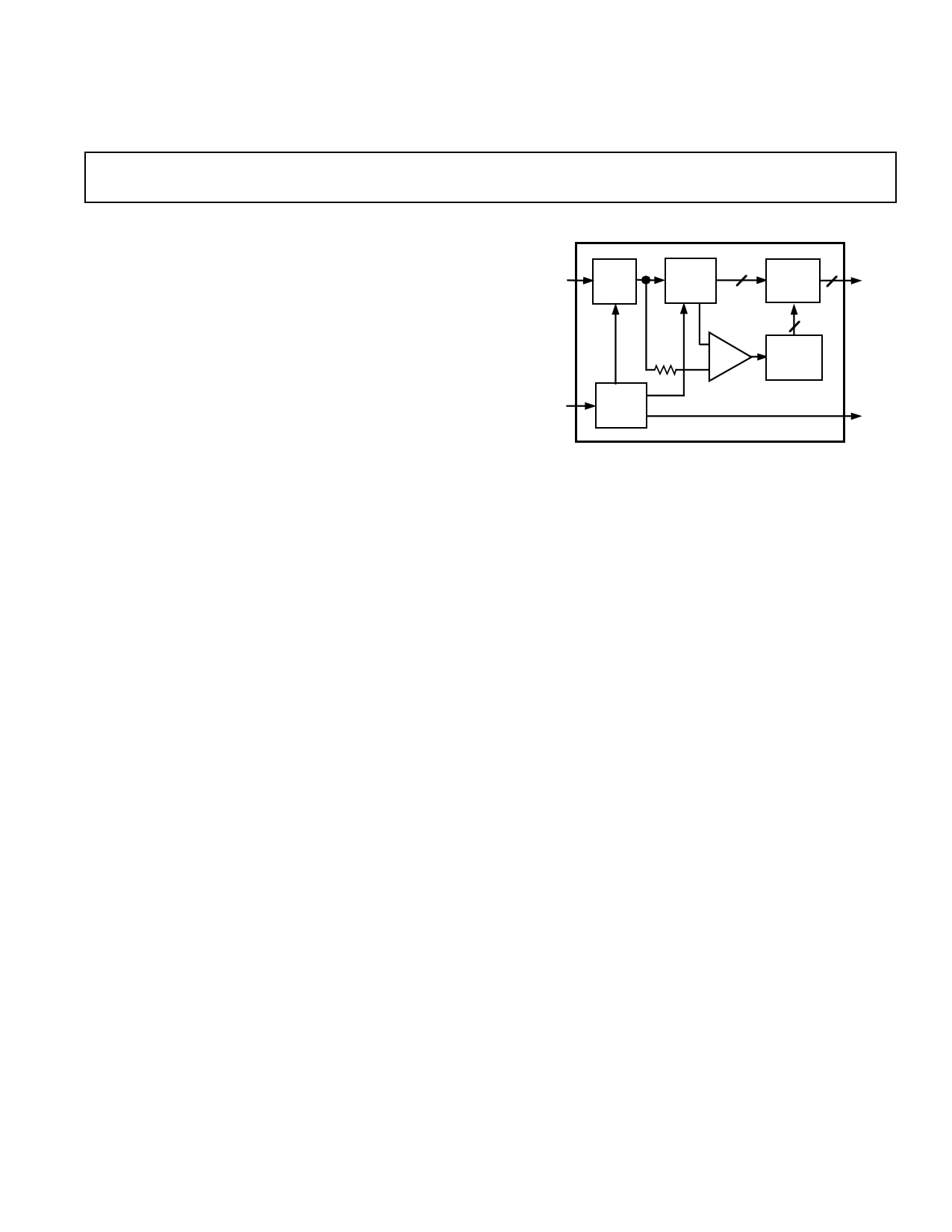
FUNCTIONAL BLOCK DIAGRAM
25.6 MSPS Conversion Speeds
On-Board T/H, References, Timing
Low Power: 3.8 W
Single 40-Pin Package
74 dB Spurious-Free Dynamic Range
ANALOG
INPUT
TRACK-
AND-
HOLD
FLASH
ADC/DAC
5
ERROR
CORR.
LOGIC
12
DIGITAL
OUTPUT
to 12 MHz AIN
8
Bipolar Input: ؎1.024 V
APPLICATIONS
Radar
Signal Intelligence
Digital Spectrum Analyzers
Medical Imaging
OElectro-Optics
ENCODE
TIMING
CIRCUITS
SUM
AMP
RESIDUE
ENCODER
AD9032
DATA
READY
BSGENERAL DESCRIPTION
OThe AD9032 is the world’s fastest 12-bit analog-to-digital con-
verter (ADC) that includes on-board T/H, voltage references,
Land timing circuits. The AD9032 uses a subranging converter
Earchitecture to achieve sample rates from dc to 25.6 MSPS. Pack-
aged in a single 40-pin hybrid, the AD9032 is pin-compatible with
TEthe AD9034, which operates at word rates up to 20 MSPS.
EVALUATION BOARD
An evaluation board which is available for the AD9032 (part
number AD9034/PCB) provides an easy and flexible method
for evaluating the ADC’s performance without (or prior to)
developing a user-specified printed circuit board. The evalua-
tion board was originally designed and used for evaluating the
AD9034 A/D converter, but is equally useful for the pin-
This ECL-compatible ADC requires only +5 V and –5.2 V sup- compatible AD9032.
plies, an analog input, and a stable ECL clock to obtain the best The board includes a reconstruction DAC, analog input ampli-
dynamic performance available in a 12-bit ADC. This kind of
fier, and digital output interface. Physically, it is 7.25 inches ϫ
performance is achieved with advanced bipolar circuits, custom 6 inches in size and uses the layout and applications information
designed and manufactured by Analog Devices. The latest in
contained in the AD9034 data sheet.
monolithic track-and-hold technology ensures accurate sam-
pling of high frequency analog inputs.
Generous space is provided near the analog input and digital
outputs of the evaluation board to support additional signal pro-
Dynamic performance has been optimized to achieve SNR of
cessing components the user may wish to add. These two proto-
64 dB and a spurious-free dynamic range (SFDR) of 74 dB for typing areas include through holes with 100-mil centers to
analog bandwidths up to 12 MHz. All units are tested for dy-
support a variety of component additions.
namic performance at a sample rate of 25.6 MSPS.
For additional operating details, a schematic of the evaluation
The AD9032 is available in either a 40-pin ceramic DIP or
board, and complete layout information, consult the data sheet
leaded flatpack. The two versions operate over an industrial
on the AD9034 A/D converter.
(–25°C to +85°C) or military (–55°C to +125°C) temperature
range.
REV. 0
Information furnished by Analog Devices is believed to be accurate and
reliable. However, no responsibility is assumed by Analog Devices for its
use, nor for any infringements of patents or other rights of third parties
which may result from its use. No license is granted by implication or
otherwise under any patent or patent rights of Analog Devices.
One Technology Way, P.O. Box 9106, Norwood, MA 02062-9106, U.S.A.
Tel: 617/329-4700
Fax: 617/326-8703
1 page 
AD9032
PIN DESCRIPTIONS
THEORY OF OPERATION
Pin Name
Description
The AD9032 is a digitally corrected subranging analog-to-digital
converter (ADC) optimized for fast sampling rates and dynamic
1
GAIN
Can be used to null out initial gain range. Refer to the block diagram on the first page. The
ADJUST
error of ADC. Normally open.
AD9032 is a vertically integrated structure consisting of a track-
and-hold (T/H) amplifier, a combined flash ADC and digital-to-
2
OFFSET
Can be used to null out initial off- analog (DAC), a summation amplifier, digital error correction
ADJUST
set error of ADC. Normally open. logic, and timing circuits. Reference circuits to generate stable
3, 5, 6, GROUND
14, 21,
22, 35, 40
All ground pins should be connect
ed together and to low-impedance
ground plane near AD9034.
DC voltages and currents that maintain the static accuracy of
the device are also included, but are not shown on the block
diagram.
Internally, the monolithic T/H (AD9101) provides fast settling
4
ANALOG Analog input to ADC, ± 1.024 V
and acquisition times while minimizing distortion introduced by
INPUT
input range; 100 Ω input resist-
ance; 7 pF input capacitance.
7, 8, 9, 15, DNC
16, 36, 37
Do not connect. Internal test
points.
10 OVERFLOW ECL-compatible output; normally
O low. High when analog input
> +FS.
B11 DATA
SREADY
OL12, 17,
20, 38
–VS
ECL-compatible output. Rising
edge of signal suitable, for exter-
nally latching D0 – D11.
–5.2 V supply voltage.
E13, 39
TE18
+VS
ENCODE
+5.0 V supply voltage.
Differential ECL convert command.
the sampling process. The unique design of the sampling bridge
allows accurate sampling of high slew rate signals with negligible
distortion. The effects of jitter and other aperture errors have
been reduced to provide dynamic performance previously un-
available in monolithic and discrete designs.
At the output of the T/H amplifier, the analog input is converted
by the first (5-bit) ADC. This 12-bit representation of the input
value is stored in the digital error correction logic. It is also con-
verted back to an analog signal by the 14-bit-accurate DAC on
the same chip with the ADC. The 32 DAC current sources are
steered directly by the outputs of the 32 input comparators on
the 5-bit ADC. This minimizes propagation delay through the
DAC, and allows the summation of the DAC signal and the held
output of the T/H to settle quickly. The hold time of the T/H is
optimized to allow sufficient settling time without sacrificing the
acquisition time necessary to acquire the next sample.
The residue signal, representing the difference between the 5-bit
conversion (DAC output) and the input signal held by the T/H,
19
ENCODE Sampling occurs on rising edge;
is amplified by the summation amplifier. During the tracking pe-
no internal terminations.
riod of the T/H, this residue signal can be much larger than the
23–34
D0–D11
ECL-compatible digital outputs;
2s complement coding.
input range of the 8-bit ADC and would saturate the output
stage of a normal amplifier. To protect the ADC and maintain
fast settling times under all conditions, the summation amplifier
is a custom design with clamping circuits that prevent satura-
PIN DESIGNATIONS
tion, limit the output voltage, and preserve settling time.
The 8-bit flash ADC determines the 7 least significant bits
DNC
DNC
GROUND
ANALOG INPUT
GROUND
1
2
3
4
5
40 GROUND
39 +VS
38 –VS
37 DNC
36 DNC
(LSBs) of the 12-bit conversion and generates a correction bit
for any small errors created by inaccuracies in the first 5-bit con-
version. This 8-bit signal and the 5-bit quantization are com-
bined to obtain a 12-bit-accurate representation of the analog
input voltage.
GROUND 6
35 GROUND
DNC 7
34 D0 (LSB)
DNC 8
33 D1
DNC 9 AD9032 32 D2
OVERFLOW 10 TOP VIEW 31 D3
DATA READY 11 (Not to Scale) 30 D4
–VS 12
29 D5
+VS 13
28 D6
GROUND 14
27 D7
DNC 15
26 D8
DNC 16
25 D9
–VS 17
24 D10
ENCODE 18
23 D11 (MSB)
ENCODE 19
22 GROUND
–VS DIGITAL 20
21 GROUND
REV. 0
–5–
5 Page | ||
| Páginas | Total 8 Páginas | |
| PDF Descargar | [ Datasheet AD9032.PDF ] | |
Hoja de datos destacado
| Número de pieza | Descripción | Fabricantes |
| AD9032 | 12-Bit 25 MSPS A/D Converter | Analog Devices |
| AD9034 | A/D CONVERTER | Analog Devices |
| Número de pieza | Descripción | Fabricantes |
| SLA6805M | High Voltage 3 phase Motor Driver IC. |
Sanken |
| SDC1742 | 12- and 14-Bit Hybrid Synchro / Resolver-to-Digital Converters. |
Analog Devices |
|
DataSheet.es es una pagina web que funciona como un repositorio de manuales o hoja de datos de muchos de los productos más populares, |
| DataSheet.es | 2020 | Privacy Policy | Contacto | Buscar |