|
|
|
PDF AD9516-1 Data sheet ( Hoja de datos )
| Número de pieza | AD9516-1 | |
| Descripción | 14-Output Clock Generator | |
| Fabricantes | Analog Devices | |
| Logotipo | ||
Hay una vista previa y un enlace de descarga de AD9516-1 (archivo pdf) en la parte inferior de esta página. Total 30 Páginas | ||
|
No Preview Available !
Data Sheet
14-Output Clock Generator with
Integrated 2.5 GHz VCO
AD9516-1
FEATURES
Low phase noise, phase-locked loop (PLL)
On-chip VCO tunes from 2.30 GHz to 2.65 GHz
External VCO/VCXO to 2.4 GHz optional
1 differential or 2 single-ended reference inputs
Reference monitoring capability
Automatic revertive and manual reference
switchover/holdover modes
Accepts LVPECL, LVDS, or CMOS references to 250 MHz
Programmable delays in path to PFD
Digital or analog lock detect, selectable
6 pairs of 1.6 GHz LVPECL outputs
Each output pair shares a 1-to-32 divider with coarse
phase delay
Additive output jitter: 225 fs rms
Channel-to-channel skew paired outputs of <10 ps
4 pairs of 800 MHz LVDS clock outputs
Each output pair shares two cascaded 1-to-32 dividers
with coarse phase delay
Additive output jitter: 275 fs rms
Fine delay adjust (Δt) on each LVDS output
Each LVDS output can be reconfigured as two 250 MHz
CMOS outputs
Automatic synchronization of all outputs on power-up
Manual output synchronization available
64-lead LFCSP
APPLICATIONS
Low jitter, low phase noise clock distribution
10/40/100 Gb/sec networking line cards, including SONET,
Synchronous Ethernet, OTU2/3/4
Forward error correction (G.710)
Clocking high speed ADCs, DACs, DDSs, DDCs, DUCs, MxFEs
High performance wireless transceivers
ATE and high performance instrumentation
GENERAL DESCRIPTION
The AD9516-11 provides a multi-output clock distribution
function with subpicosecond jitter performance, along with an on-
chip PLL and VCO. The on-chip VCO tunes from 2.30 GHz to
2.65 GHz. Optionally, an external VCO/VCXO of up to 2.4 GHz
can be used.
The AD9516-1 emphasizes low jitter and phase noise to
maximize data converter performance, and it can benefit other
applications with demanding phase noise and jitter requirements.
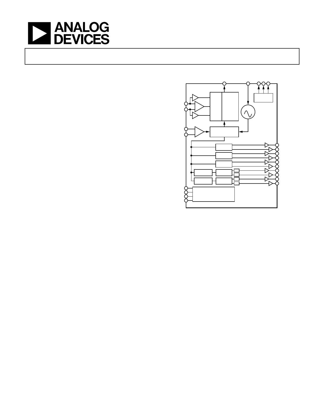
FUNCTIONAL BLOCK DIAGRAM
CP LF
REFIN
REF1
REF2
STATUS
MONITOR
VCO
CLK
DIVIDER
AND MUXs
DIV/Φ
LVPECL
DIV/Φ
LVPECL
DIV/Φ
DIV/Φ
DIV/Φ
DIV/Φ
DIV/Φ
LVPECL
Δt
Δt
LVDS/CMOS
Δt
Δt
LVDS/CMOS
SERIAL CONTROL PORT
AND
DIGITAL LOGIC
AD9516-1
OUT0
OUT1
OUT2
OUT3
OUT4
OUT5
OUT6
OUT7
OUT8
OUT9
Figure 1.
The AD9516-1 features six LVPECL outputs (in three pairs) and
four LVDS outputs (in two pairs). Each LVDS output can be
reconfigured as two CMOS outputs. The LVPECL outputs
operate to 1.6 GHz, the LVDS outputs operate to 800 MHz, and
the CMOS outputs operate to 250 MHz.
Each pair of outputs has dividers that allow both the divide ratio
and coarse delay (or phase) to be set. The range of division for
the LVPECL outputs is 1 to 32. The LVDS/CMOS outputs allow
a range of divisions up to a maximum of 1024.
The AD9516-1 is available in a 64-lead LFCSP and can be
operated from a single 3.3 V supply. An external VCO, which
requires an extended voltage range, can be accommodated by
connecting the charge pump supply (VCP) to 5 V. A separate
LVPECL power supply can be from 2.5 V to 3.3 V (nominal).
The AD9516-1 is specified for operation over the industrial
range of −40°C to +85°C.
1 AD9516 is used throughout to refer to all the members of the AD9516 family.
However, when AD9516-1 is used, it refers to that specific member of the
AD9516 family.
Rev. C
Document Feedback
Information furnished by Analog Devices is believed to be accurate and reliable. However, no
responsibilityisassumedbyAnalogDevices for itsuse,nor foranyinfringementsofpatentsor other
rights of third parties that may result from its use. Specifications subject to change without notice. No
license is granted by implication or otherwise under any patent or patent rights of Analog Devices.
Trademarksandregisteredtrademarksarethepropertyoftheirrespectiveowners.
One Technology Way, P.O. Box 9106, Norwood, MA 02062-9106, U.S.A.
Tel: 781.329.4700 ©2007–2013 Analog Devices, Inc. All rights reserved.
Technical Support
www.analog.com
1 page 
AD9516-1
Data Sheet
SPECIFICATIONS
Typical is given for VS = VS_LVPECL = 3.3 V ± 5%; VS ≤ VCP ≤ 5.25 V; TA = 25°C; RSET = 4.12 kΩ; CPRSET = 5.1 kΩ, unless otherwise noted.
Minimum and maximum values are given over full VS and TA (−40°C to +85°C) variation.
POWER SUPPLY REQUIREMENTS
Table 1.
Parameter
VS
VS_LVPECL
VCP
RSET Pin Resistor
CPRSET Pin Resistor
BYPASS Pin Capacitor
Min
3.135
2.375
VS
2.7
Typ
3.3
4.12
5.1
Max
3.465
VS
5.25
10
Unit
V
V
V
kΩ
kΩ
220 nF
Test Conditions/Comments
3.3 V ± 5%
Nominally 2.5 V to 3.3 V ± 5%
Nominally 3.3 V to 5.0 V ± 5%
Sets internal biasing currents; connect to ground
Sets internal CP current range, nominally 4.8 mA (CP_lsb = 600 µA);
actual current can be calculated by: CP_lsb = 3.06/CPRSET;
connect to ground
Bypass for internal LDO regulator; necessary for LDO stability;
connect to ground
PLL CHARACTERISTICS
Table 2.
Parameter
VCO (ON-CHIP)
Frequency Range
VCO Gain (KVCO)
Tuning Voltage (VT)
Frequency Pushing (Open-Loop)
Phase Noise at 100 kHz Offset
Phase Noise at 1 MHz Offset
REFERENCE INPUTS
Differential Mode (REFIN, REFIN)
Input Frequency
Input Sensitivity
Self-Bias Voltage, REFIN
Self-Bias Voltage, REFIN
Input Resistance, REFIN
Input Resistance, REFIN
Dual Single-Ended Mode (REF1, REF2)
Input Frequency (AC-Coupled)
Input Frequency (DC-Coupled)
Input Sensitivity (AC-Coupled)
Input Logic High
Input Logic Low
Input Current
Input Capacitance
PHASE/FREQUENCY DETECTOR (PFD)
PFD Input Frequency
Antibacklash Pulse Width
Min Typ Max Unit
Test Conditions/Comments
2300
0.5
50
1
−105
−124
2650
VCP −
0.5
MHz
MHz/V
V
MHz/V
dBc/Hz
dBc/Hz
See Figure 15
See Figure 10
VCP ≤ VS when using internal VCO; outside of this range, the CP
spurs may increase due to CP up/down mismatch
f = 2475 MHz
f = 2475 MHz
0
250
1.35 1.60
1.30 1.50
4.0 4.8
4.4 5.3
20
0
0.8
2.0
−100
2
250
1.75
1.60
5.9
6.4
250
250
0.8
+100
MHz
mV p-p
V
V
kΩ
kΩ
MHz
MHz
V p-p
V
V
µA
pF
Differential mode (can accommodate single-ended input by ac
grounding undriven input)
Frequencies below about 1 MHz should be dc-coupled;
be careful to match VCM (self-bias voltage)
PLL figure of merit (FOM) increases with increasing slew rate;
see Figure 14
Self-bias voltage of REFIN1
Self-bias voltage of REFIN1
Self-biased1
Self-biased1
Two single-ended CMOS-compatible inputs
Slew rate > 50 V/µs
Slew rate > 50 V/µs; CMOS levels
Should not exceed VS p-p
Each pin, REFIN/REFIN (REF1/REF2)
100 MHz Antibacklash pulse width = 1.3 ns, 2.9 ns
45 MHz Antibacklash pulse width = 6.0 ns
1.3 ns Register 0x017[1:0] = 01b
2.9 ns Register 0x017[1:0] = 00b; Register 0x017[1:0] = 11b
6.0 ns Register 0x017[1:0] = 10b
Rev. C | Page 4 of 80
5 Page 
AD9516-1
Data Sheet
CLOCK OUTPUT ABSOLUTE TIME JITTER (CLOCK GENERATION USING INTERNAL VCO)
Table 8.
Parameter
Min Typ Max Unit Test Conditions/Comments
LVPECL OUTPUT ABSOLUTE TIME JITTER
Application example based on a typical
setup where the reference source is clean,
so a wider PLL loop bandwidth is used;
reference = 15.36 MHz; R = 1
VCO = 2.46 GHz; LVPECL = 491.52 MHz; PLL LBW = 55 kHz
142
fs rms Integration BW = 200 kHz to 10 MHz
370 fs rms Integration BW = 12 kHz to 20 MHz
VCO = 2.46 GHz; LVPECL = 122.88 MHz; PLL LBW = 55 kHz
145
fs rms Integration BW = 200 kHz to 10 MHz
356 fs rms Integration BW = 12 kHz to 20 MHz
VCO = 2.46 GHz; LVPECL = 61.44 MHz; PLL LBW = 55 kHz 195 fs rms Integration BW = 200 kHz to 10 MHz
402 fs rms Integration BW = 12 kHz to 20 MHz
CLOCK OUTPUT ABSOLUTE TIME JITTER (CLOCK CLEANUP USING INTERNAL VCO)
Table 9.
Parameter
Min Typ Max Unit Test Conditions/Comments
LVPECL OUTPUT ABSOLUTE TIME JITTER
Application example based on a typical
setup where the reference source is jittery,
so a narrower PLL loop bandwidth is used;
reference = 10.0 MHz; R = 20
VCO = 2.49 GHz; LVPECL = 622.08 MHz; PLL LBW = 125 Hz
745
fs rms Integration BW = 12 kHz to 20 MHz
VCO = 2.49 GHz; LVPECL = 155.52 MHz; PLL LBW = 125 Hz
712
fs rms Integration BW = 12 kHz to 20 MHz
VCO = 2.46 GHz; LVPECL = 122.88 MHz; PLL LBW = 125 Hz
700
fs rms Integration BW = 12 kHz to 20 MHz
CLOCK OUTPUT ABSOLUTE TIME JITTER (CLOCK GENERATION USING EXTERNAL VCXO)
Table 10.
Parameter
LVPECL OUTPUT ABSOLUTE TIME JITTER
LVPECL = 245.76 MHz; PLL LBW = 125 Hz
LVPECL = 122.88 MHz; PLL LBW = 125 Hz
LVPECL = 61.44 MHz; PLL LBW = 125 Hz
Min Typ Max Unit Test Conditions/Comments
Application example based on a typical
setup using an external 245.76 MHz VCXO
(Toyocom TCO-2112); reference = 15.36 MHz;
R=1
54 fs rms Integration BW = 200 kHz to 5 MHz
77 fs rms Integration BW = 200 kHz to 10 MHz
109 fs rms Integration BW = 12 kHz to 20 MHz
79 fs rms Integration BW = 200 kHz to 5 MHz
114 fs rms Integration BW = 200 kHz to 10 MHz
163 fs rms Integration BW = 12 kHz to 20 MHz
124 fs rms Integration BW = 200 kHz to 5 MHz
176 fs rms Integration BW = 200 kHz to 10 MHz
259 fs rms Integration BW = 12 kHz to 20 MHz
Rev. C | Page 10 of 80
11 Page | ||
| Páginas | Total 30 Páginas | |
| PDF Descargar | [ Datasheet AD9516-1.PDF ] | |
Hoja de datos destacado
| Número de pieza | Descripción | Fabricantes |
| AD9516-0 | 14-Output Clock Generator | Analog Devices |
| AD9516-1 | 14-Output Clock Generator | Analog Devices |
| AD9516-2 | 14-Output Clock Generator | Analog Devices |
| AD9516-3 | 14-Output Clock Generator | Analog Devices |
| Número de pieza | Descripción | Fabricantes |
| SLA6805M | High Voltage 3 phase Motor Driver IC. |
Sanken |
| SDC1742 | 12- and 14-Bit Hybrid Synchro / Resolver-to-Digital Converters. |
Analog Devices |
|
DataSheet.es es una pagina web que funciona como un repositorio de manuales o hoja de datos de muchos de los productos más populares, |
| DataSheet.es | 2020 | Privacy Policy | Contacto | Buscar |