|
|
|
PDF AD9522-4 Data sheet ( Hoja de datos )
| Número de pieza | AD9522-4 | |
| Descripción | 12 LVDS/24 CMOS Output Clock Generator | |
| Fabricantes | Analog Devices | |
| Logotipo | ||
Hay una vista previa y un enlace de descarga de AD9522-4 (archivo pdf) en la parte inferior de esta página. Total 30 Páginas | ||
|
No Preview Available !
Data Sheet
12 LVDS/24 CMOS Output Clock Generator
with Integrated 1.6 GHz VCO
AD9522-4
FEATURES
Low phase noise, phase-locked loop (PLL)
On-chip voltage controlled oscillator (VCO) tunes from
1.4 GHz to 1.8 GHz
Supports external 3.3 V/5 V VCO/VCXO to 2.4 GHz
1 differential or 2 single-ended reference inputs
Accepts CMOS, LVPECL, or LVDS references to 250 MHz
Accepts 16.62 MHz to 33.3 MHz crystal for reference input
Optional reference clock doubler
Reference monitoring capability
Revertive automatic and manual reference switchover/
holdover modes
Glitch-free switchover between references
Automatic recovery from holdover
Digital or analog lock detect, selectable
Optional zero delay operation
Twelve 800 MHz LVDS outputs divided into 4 groups
Each group of 3 has a 1-to-32 divider with phase delay
Additive output jitter as low as 242 fs rms
Channel-to-channel skew grouped outputs <60 ps
Each LVDS output can be configured as 2 CMOS outputs
(for fOUT ≤ 250 MHz)
Automatic synchronization of all outputs on power-up
Manual synchronization of outputs as needed
SPI- and I²C-compatible serial control port
64-lead LFCSP
Nonvolatile EEPROM stores configuration settings
APPLICATIONS
Low jitter, low phase noise clock distribution
Clock generation and translation for SONET, 10Ge, 10G FC,
and other 10 Gbps protocols
Forward error correction (G.710)
Clocking high speed ADCs, DACs, DDSs, DDCs, DUCs, MxFEs
High performance wireless transceivers
ATE and high performance instrumentation
Broadband infrastructures
GENERAL DESCRIPTION
The AD9522-41 provides a multioutput clock distribution
function with subpicosecond jitter performance, along with an
on-chip PLL and VCO. The on-chip VCO tunes from 1.4 GHz to
1.8 GHz. An external 3.3 V/5 V VCO/VCXO of up to 2.4 GHz
can also be used.
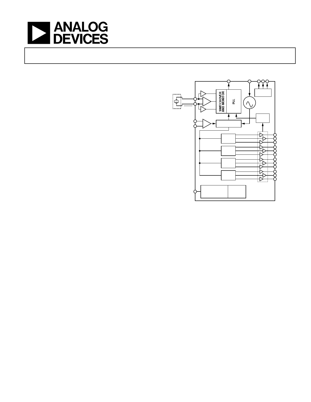
FUNCTIONAL BLOCK DIAGRAM
CP LF
OPTIONAL
REFIN
REFIN
CLK
REF1
REF2
DIVIDER
AND MUXES
DIV/Φ
VCO
STATUS
MONITOR
ZERO
DELAY
LVDS/
CMOS
DIV/Φ
DIV/Φ
DIV/Φ
SPI/I2C CONTROL
PORT AND
EEPROM
DIGITAL LOGIC
AD9522
OUT0
OUT1
OUT2
OUT3
OUT4
OUT5
OUT6
OUT7
OUT8
OUT9
OUT10
OUT11
Figure 1.
The AD9522 serial interface supports both SPI and I2C® ports.
An in-package EEPROM can be programmed through the
serial interface and store user-defined register settings for
power-up and chip reset.
The AD9522 features 12 LVDS outputs in four groups. Any of
the 800 MHz LVDS outputs can be reconfigured as two 250 MHz
CMOS outputs.
Each group of outputs has a divider that allows both the divide
ratio (from 1 to 32) and the phase (coarse delay) to be set.
The AD9522 is available in a 64-lead LFCSP and can be operated
from a single 3.3 V supply. The external VCO can have an
operating voltage up to 5.5 V.
The AD9522 is specified for operation over the standard industrial
range of −40°C to +85°C.
The AD9520-4 is an equivalent device to the AD9522-4 featuring
LVPECL/CMOS drivers instead of LVDS/CMOS drivers.
1 The AD9522 is used throughout this data sheet to refer to all the members of the AD9522 family. However, when AD9522-4 is used, it is referring to that specific
member of the AD9522 family.
Rev. A
Document Feedback
Information furnished by Analog Devices is believed to be accurate and reliable. However, no
responsibility is assumed by Analog Devices for its use, nor for any infringements of patents or other
rights of third parties that may result from its use. Specifications subject to change without notice. No
license is granted by implication or otherwise under any patent or patent rights of Analog Devices.
Trademarksandregisteredtrademarksarethepropertyoftheirrespectiveowners.
One Technology Way, P.O. Box 9106, Norwood, MA 02062-9106, U.S.A.
Tel: 781.329.4700 ©2008–2015 Analog Devices, Inc. All rights reserved.
Technical Support
www.analog.com
1 page 
AD9522-4
REVISION HISTORY
3/15—Rev. 0 to Rev. A
Changes to Features Section............................................................ 1
Changes to Table 1 and Table 2....................................................... 5
Change to Input Frequency Parameter, Table 3 ........................... 8
Changes to Table 4............................................................................ 8
Changes to SDIO, SDO (Outputs) Parameter, Test
Conditions/Comments Column, Table 13 .................................. 13
Changes to Table 17........................................................................ 15
Change to VCP Supply Parameter, Table 18 ............................... 16
Change to Junction Temperature Parameter, Table 19 .............. 17
Changes to Pin 4 Description Column, Table 21 and Pin 22
Description Column, Table 21...................................................... 18
Removed Figure 13; Renumbered Sequentially.......................... 21
Added Test Circuits Section .......................................................... 26
Moved Figure 33 and Figure 34 .................................................... 26
Changes to Figure 33 and Figure 34............................................. 26
Changes to Mode 0: Internal VCO and Clock Distribution
Section.............................................................................................. 29
Deleted Configuration and Register Settings Section ............... 29
Changes to Figure 36...................................................................... 30
Changes to Figure 37...................................................................... 32
Changes to Figure 38...................................................................... 34
Changes to Configuration of the PLL Section and Charge Pump
(CP) Section .................................................................................... 35
Changes to On-Chip VCO Section, Figure 40, and PLL
Reference Inputs Section ............................................................... 36
Added Figure 42 and Figure 43; Renumbered Sequentially ..... 36
Changes to Reference Switchover Section................................... 37
Changes to Prescaler Section, A and B Counters Section, R and
N Divider Delays, and Table 29 .................................................... 38
Changes to Current Source Digital Lock Detect (CSDLD)
Section.............................................................................................. 39
Data Sheet
Changes to External VCXO/VCO Clock Input (CLK/CLK)
Section and Holdover Section ...................................................... 40
Changes to Frequency Status Monitors Section and VCO
Calibration Section......................................................................... 42
Changes to Figure 49 Caption ...................................................... 43
Added Table 31; Renumbered Sequentially ................................ 44
Changes to Zero Delay Operation Section and Internal Zero
Delay Mode Section ....................................................................... 45
Changes to Clock Distribution Section....................................... 46
Changes to VCO Divider Section and Channel Frequency
Division (0, 1, 2, and 3) Section.................................................... 47
Added Channel Divider Maximum Frequency Section............ 47
Changes to Duty Cycle and Duty-Cycle Correction Section and
Table 37 ............................................................................................ 48
Changes to Synchronizing the Outputs—SYNC Function
Section.............................................................................................. 49
Changes to Power-On Reset Section, Hardware Reset via
the RESET Pin Section, and Soft Reset via the Serial Port Section 51
Changes to Pin Descriptions Section and SPI Mode Operation
Section.............................................................................................. 56
Changes to SPI Instruction Word (16 Bits) Section .................. 57
Changes to Figure 66, Figure 67 Caption, and Figure 68.......... 58
Changes to EEPROM Operation Section.................................... 60
Changes to Table 49 ....................................................................... 64
Changes to Table 50 and Table 51 ................................................ 68
Changes to Table 53 ....................................................................... 69
Changes to Table 55 ....................................................................... 77
Change to Table 58 ......................................................................... 81
Change to Frequency Planning Using the AD9522 Section..... 82
Updated Outline Dimensions....................................................... 84
10/08—Revision 0: Initial Version
Rev. A | Page 4 of 84
5 Page 
AD9522-4
Data Sheet
CLOCK OUTPUT ADDITIVE PHASE NOISE (DISTRIBUTION ONLY; VCO DIVIDER NOT USED)
Table 6.
Parameter
CLK-TO-LVDS ADDITIVE PHASE NOISE
CLK = 1.6 GHz, Output = 800 MHz
Divider = 2
At 10 Hz Offset
At 100 Hz Offset
At 1 kHz Offset
At 10 kHz Offset
At 100 kHz Offset
At 1 MHz Offset
At 10 MHz Offset
At 100 MHz Offset
CLK = 1 GHz, Output = 200 MHz
Divider = 5
At 10 Hz Offset
At 100 Hz Offset
At 1 kHz Offset
At 10 kHz Offset
At 100 kHz Offset
At 1 MHz Offset
>10 MHz Offset
CLK-TO-CMOS ADDITIVE PHASE NOISE
CLK = 1 GHz, Output = 500 MHz
Divider = 2
At 10 Hz Offset
At 100 Hz Offset
At 1 kHz Offset
At 10 kHz Offset
At 100 kHz Offset
At 1 MHz Offset
>10 MHz Offset
CLK = 1 GHz, Output = 50 MHz
Divider = 20
At 10 Hz Offset
At 100 Hz Offset
At 1 kHz Offset
At 10 kHz Offset
At 100 kHz Offset
At 1 MHz Offset
>10 MHz Offset
Min Typ Max Unit
Test Conditions/Comments
Distribution section only; does not include PLL and VCO
Input slew rate > 1 V/ns
−100
−110
−117
−126
−134
−137
−147
−148
dBc/Hz
dBc/Hz
dBc/Hz
dBc/Hz
dBc/Hz
dBc/Hz
dBc/Hz
dBc/Hz
Input slew rate > 1 V/ns
−111
−123
−132
−141
−146
−150
−156
dBc/Hz
dBc/Hz
dBc/Hz
dBc/Hz
dBc/Hz
dBc/Hz
dBc/Hz
Distribution section only; does not include PLL and VCO
Input slew rate > 1 V/ns
−102
−114
−122
−129
−135
−140
−150
dBc/Hz
dBc/Hz
dBc/Hz
dBc/Hz
dBc/Hz
dBc/Hz
dBc/Hz
Input slew rate > 1 V/ns
−125
−136
−144
−152
−157
−160
−164
dBc/Hz
dBc/Hz
dBc/Hz
dBc/Hz
dBc/Hz
dBc/Hz
dBc/Hz
Rev. A | Page 10 of 84
11 Page | ||
| Páginas | Total 30 Páginas | |
| PDF Descargar | [ Datasheet AD9522-4.PDF ] | |
Hoja de datos destacado
| Número de pieza | Descripción | Fabricantes |
| AD9522-0 | 12 LVDS/24 CMOS Output Clock Generator | Analog Devices |
| AD9522-1 | 12 LVDS/24 CMOS Output Clock Generator | Analog Devices |
| AD9522-2 | 12 LVDS/24 CMOS Output Clock Generator | Analog Devices |
| AD9522-3 | 12 LVDS/24 CMOS Output Clock Generator | Analog Devices |
| Número de pieza | Descripción | Fabricantes |
| SLA6805M | High Voltage 3 phase Motor Driver IC. |
Sanken |
| SDC1742 | 12- and 14-Bit Hybrid Synchro / Resolver-to-Digital Converters. |
Analog Devices |
|
DataSheet.es es una pagina web que funciona como un repositorio de manuales o hoja de datos de muchos de los productos más populares, |
| DataSheet.es | 2020 | Privacy Policy | Contacto | Buscar |