|
|
|
PDF AD8052 Data sheet ( Hoja de datos )
| Número de pieza | AD8052 | |
| Descripción | Rail-to-Rail Amplifiers | |
| Fabricantes | Analog Devices | |
| Logotipo | ||
Hay una vista previa y un enlace de descarga de AD8052 (archivo pdf) en la parte inferior de esta página. Total 24 Páginas | ||
|
No Preview Available !
FEATURES
High speed and fast settling on 5 V
110 MHz, −3 dB bandwidth (G = +1) (AD8051/AD8052)
150 MHz, −3 dB bandwidth (G = +1) (AD8054)
145 V/μs slew rate
50 ns settling time to 0.1%
Single-supply operation
Output swings to within 25 mV of either rail
Input voltage range: −0.2 V to +4 V; VS = 5 V
Video specifications (G = +2)
0.1 dB gain flatness: 20 MHz; RL = 150 Ω
Differential gain/phase: 0.03%/0.03°
Low distortion
−80 dBc total harmonic @ 1 MHz, RL = 100 Ω
Outstanding load drive capability
Drives 45 mA, 0.5 V from supply rails (AD8051/AD8052)
Drives 50 pF capacitive load (G = +1) (AD8051/AD8052)
Low power: 2.75 mA/amplifier (AD8054)
Low power: 4.4 mA/amplifier (AD8051/AD8052)
APPLICATIONS
Active filters
Analog-to-digital drivers
Clock buffer
Consumer video
Professional cameras
CCD imaging systems
CD/DVD ROMs
GENERAL DESCRIPTION
The AD8051 (single), AD8052 (dual), and AD8054 (quad) are
low cost, high speed, voltage feedback amplifiers. The amplifiers
operate on +3 V, +5 V, or ±5 V supplies at low supply current.
They have true single-supply capability with an input voltage
range extending 200 mV below the negative rail and within 1 V
of the positive rail.
Despite their low cost, the AD8051/AD8052/AD8054 provide
excellent overall performance and versatility. The output voltage
swings to within 25 mV of each rail, providing maximum output
dynamic range with excellent overdrive recovery.
Rev. J
Information furnished by Analog Devices is believed to be accurate and reliable. However, no
responsibility is assumed by Analog Devices for its use, nor for any infringements of patents or other
rights of third parties that may result from its use. Specifications subject to change without notice. No
license is granted by implication or otherwise under any patent or patent rights of Analog Devices.
Trademarksandregisteredtrademarksarethepropertyoftheirrespectiveowners.
Low Cost, High Speed,
Rail-to-Rail Amplifiers
AD8051/AD8052/AD8054
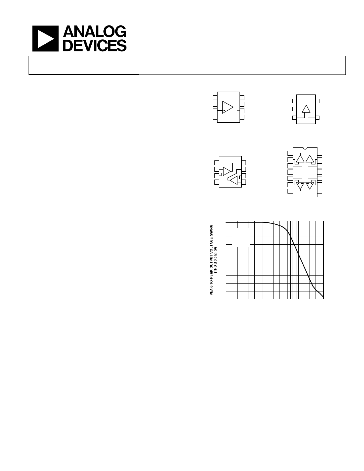
PIN CONNECTIONS (TOP VIEWS)
NC 1
–IN 2
+IN 3
–VS 4
AD8051
8 NC
7 +VS
6 VOUT
5 NC
NC = NO CONNECT
Figure 1. SOIC-8 (R)
AD8051
VOUT 1
5 +VS
–VS 2
+–
+IN 3
4 –IN
Figure 2. SOT-23-5 (RJ)
OUT1 1
–IN1 2
+IN1 3
–VS 4
AD8052
–
+
–
+
8 +VS
7 OUT
6 –IN2
5 +IN2
OUT A 1
–IN A 2
+IN A 3
V+ 4
+IN B 5
–IN B 6
OUT B 7
AD8054
14 OUT D
13 –IN D
12 +IN D
11 V–
10 +IN C
9 –IN C
8 OUT C
Figure 3. SOIC (R-8) and MSOP (RM-8) Figure 4. SOIC (R-14) and TSSOP (RU-14)
5.0
4.5 VS = 5V
4.0 G = –1
RF = 2kΩ
3.5 RL = 2kΩ
3.0
2.5
2.0
1.5
1.0
0.5
0
0.1 1 10 50
FREQUENCY (MHz)
Figure 5. Low Distortion Rail-to-Rail Output Swing
The AD8051/AD8052/AD8054 are well suited for video
electronics, cameras, video switchers, or any high speed portable
equipment. Low distortion and fast settling make them ideal for
active filter applications.
The AD8051/AD8052 in the 8-lead SOIC, the AD8052 in the
MSOP, the AD8054 in the 14-lead SOIC, and the 14-lead TSSOP
packages are available in the extended temperature range of
−40°C to +125°C.
One Technology Way, P.O. Box 9106, Norwood, MA 02062-9106, U.S.A.
Tel: 781.329.4700
www.analog.com
Fax: 781.461.3113
©2009 Analog Devices, Inc. All rights reserved.
1 page 
AD8051/AD8052/AD8054
@ TA = 25°C, VS = 3 V, RL = 2 kΩ to 1.5 V, unless otherwise noted.
Table 2.
Parameter
DYNAMIC PERFORMANCE
−3 dB Small Signal Bandwidth
Bandwidth for 0.1 dB Flatness
Slew Rate
Full Power Response
Settling Time to 0.1%
NOISE/DISTORTION PERFORMANCE
Total Harmonic Distortion1
Input Voltage Noise
Input Current Noise
Differential Gain Error (NTSC)
Differential Phase Error (NTSC)
Crosstalk
DC PERFORMANCE
Input Offset Voltage
Offset Drift
Input Bias Current
Input Offset Current
Open-Loop Gain
INPUT CHARACTERISTICS
Input Resistance
Input Capacitance
Input Common-Mode Voltage Range
Common-Mode Rejection Ratio
Conditions
G = +1, VOUT = 0.2 V p-p
G = −1, +2, VOUT =
0.2 V p-p
G = +2, VOUT = 0.2 V p-p,
RL = 150 Ω to 2.5 V
RF = 402 Ω (AD8051A/
AD8052A)
RF = 200 Ω (AD8054A)
G = −1, VOUT = 2 V step
G = +1, VOUT = 1 V p-p
G = −1, VOUT = 2 V step
fC = 5 MHz, VOUT = 2 V p-p,
G = −1, RL = 100 Ω to 1.5 V
f = 10 kHz
f = 10 kHz
G = +2, VCM = 1 V
RL = 150 Ω to 1.5 V
RL = 1 kΩ to 1.5 V
G = +2, VCM = 1 V
RL = 150 Ω to 1.5 V
RL = 1 kΩ to 1.5 V
f = 5 MHz, G = +2
TMIN − TMAX
TMIN − TMAX
RL = 2 kΩ
TMIN − TMAX
RL = 150 Ω
TMIN − TMAX
VCM = 0 V to 1.5 V
AD8051A/AD8052A
Min Typ Max
70 110
50
17
90 135
65
55
−47
16
600
0.11
0.09
0.24
0.10
−60
1.6 10
25
10
1.3 2.6
3.25
0.15 0.8
80 96
94
74 82
76
290
1.4
−0.2 to
+2
72 88
AD8054A
Min Typ
Max Unit
80 135
65
MHz
MHz
10
110 150
85
55
MHz
MHz
V/μs
MHz
ns
−48 dB
16 nV/√Hz
600 fA/√Hz
0.13 %
0.09 %
0.3 Degrees
0.1 Degrees
−60 dB
1.6
15
2
0.2
80 96
94
72 80
76
12 mV
30 mV
μV/°C
4.5 μA
4.5 μA
1.2 μA
dB
dB
dB
dB
300
1.5
−0.2 to
+2
70 86
kΩ
pF
V
dB
Rev. J | Page 5 of 24
5 Page 
6.3
6.2
6.1
6.0
5.9
5.8
5.7
5.6
VS = 5V
G = +2
5.5 RL = 150Ω
RF = 806Ω
5.4 VOUT = 0.2V p-p
5.3
0.1
1 10
FREQUENCY (MHz)
100
Figure 13. AD8051/AD8052 0.1 dB Gain Flatness vs. Frequency; G = +2
9
8
VS = +5V
VOUT = 2V p-p
7
6
5
4
3
2
VS AS SHOWN
G = +2
VS = ±5V
VOUT = 4V p-p
1
RF = 2kΩ
RL = 2kΩ
0 VOUT AS SHOWN
–1
0.1
1 10 100 500
FREQUENCY (MHz)
Figure 14. AD8051/AD8052 Large Signal Frequency Response; G = +2
80
70 VS = 5V
RL = 2kΩ
60
50
40
GAIN
30
0
20
PHASE
10
50° PHASE
MARGIN
–45
–90
0 –135
–10 –180
–20
0.01
0.1 1 10
FREQUENCY (MHz)
100 500
Figure 15. AD8051/AD8052 Open-Loop Gain and Phase vs. Frequency
AD8051/AD8052/AD8054
6.3
6.2
6.1
6.0
5.9
5.8
5.7
5.6
VS = 5V
RF = 200Ω
5.5 RL = 150Ω
G = +2
5.4 VOUT = 0.2V p-p
5.3
1
10
FREQUENCY (MHz)
100
Figure 16. AD8054 0.1 dB Gain Flatness vs. Frequency; G = +2
9
8 VS = +5V
VOUT = 2V p-p
7
6
5
4 VS = ±5V
3 VOUT = 4V p-p
2
VS AS SHOWN
G = +2
1 RF = 2kΩ
RL = 2kΩ
0 VOUT AS SHOWN
–1
0.1
1 10 100 500
FREQUENCY (MHz)
Figure 17. AD8054 Large Signal Frequency Response; G = +2
80
70 VS = 5V
RL = 2kΩ
60 CL = 5pF
50
40 GAIN
30
180
20 135
PHASE
45° PHASE
10 MARGIN 90
0 45
–10 0
–20
30k 100k
1M 10M
FREQUENCY (Hz)
100M 500M
Figure 18. AD8054 Open-Loop Gain and Phase Margin vs. Frequency
Rev. J | Page 11 of 24
11 Page | ||
| Páginas | Total 24 Páginas | |
| PDF Descargar | [ Datasheet AD8052.PDF ] | |
Hoja de datos destacado
| Número de pieza | Descripción | Fabricantes |
| AD805 | Data Retiming Phase-Locked Loop | Analog Devices |
| AD8051 | Rail-to-Rail Amplifiers | Analog Devices |
| AD8052 | Rail-to-Rail Amplifiers | Analog Devices |
| AD8054 | Rail-to-Rail Amplifiers | Analog Devices |
| Número de pieza | Descripción | Fabricantes |
| SLA6805M | High Voltage 3 phase Motor Driver IC. |
Sanken |
| SDC1742 | 12- and 14-Bit Hybrid Synchro / Resolver-to-Digital Converters. |
Analog Devices |
|
DataSheet.es es una pagina web que funciona como un repositorio de manuales o hoja de datos de muchos de los productos más populares, |
| DataSheet.es | 2020 | Privacy Policy | Contacto | Buscar |