|
|
|
PDF AD844 Data sheet ( Hoja de datos )
| Número de pieza | AD844 | |
| Descripción | Monolithic Op Amp | |
| Fabricantes | Analog Devices | |
| Logotipo | ||
Hay una vista previa y un enlace de descarga de AD844 (archivo pdf) en la parte inferior de esta página. Total 21 Páginas | ||
|
No Preview Available !
FEATURES
Wide bandwidth
60 MHz at gain of −1
33 MHz at gain of −10
Slew rate: 2000 V/μs
20 MHz full power bandwidth, 20 V p-p, RL = 500 Ω
Fast settling: 100 ns to 0.1% (10 V step)
Differential gain error: 0.03% at 4.4 MHz
Differential phase error: 0.16° at 4.4 MHz
Low offset voltage: 150 μV maximum (B Grade)
Low quiescent current: 6.5 mA
Available in tape and reel in accordance with
EIA-481-A standard
APPLICATIONS
Flash ADC input amplifiers
High speed current DAC interfaces
Video buffers and cable drivers
Pulse amplifiers
GENERAL DESCRIPTION
The AD844 is a high speed monolithic operational amplifier
fabricated using the Analog Devices, Inc., junction isolated
complementary bipolar (CB) process. It combines high band-
width and very fast large signal response with excellent dc
performance. Although optimized for use in current-to-voltage
applications and as an inverting mode amplifier, it is also suitable
for use in many noninverting applications.
The AD844 can be used in place of traditional op amps, but its
current feedback architecture results in much better ac perfor-
mance, high linearity, and an exceptionally clean pulse response.
This type of op amp provides a closed-loop bandwidth that is
determined primarily by the feedback resistor and is almost
independent of the closed-loop gain. The AD844 is free from
the slew rate limitations inherent in traditional op amps and
other current-feedback op amps. Peak output rate of change can
be over 2000 V/μs for a full 20 V output step. Settling time is
typically 100 ns to 0.1%, and essentially independent of gain.
The AD844 can drive 50 Ω loads to ±2.5 V with low distortion
and is short-circuit protected to 80 mA.
The AD844 is available in four performance grades and three
package options. In the 16-lead SOIC (RW) package, the AD844J
is specified for the commercial temperature range of 0°C to 70°C.
Rev. F
Information furnished by Analog Devices is believed to be accurate and reliable. However, no
responsibility is assumed by Analog Devices for its use, nor for any infringements of patents or other
rights of third parties that may result from its use. Specifications subject to change without notice. No
license is granted by implication or otherwise under any patent or patent rights of Analog Devices.
Trademarksandregisteredtrademarksarethepropertyoftheirrespectiveowners.
60 MHz 2000 V/μs
Monolithic Op Amp
AD844
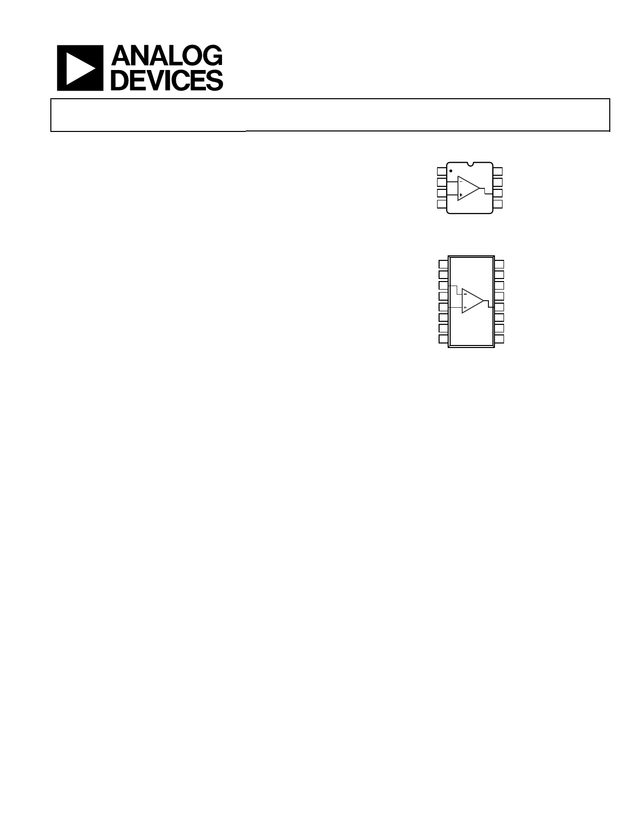
FUNCTIONAL BLOCK DIAGRAMS
NULL 1
–IN 2
+IN 3
–VS 4
AD844
8 NULL
7 +VS
6 OUTPUT
5 TZ
TOP VIEW
(Not to Scale)
Figure 1. 8-Lead PDIP (N) and 8-Lead CERDIP (Q) Packages
NC 1
16 NC
OFFSETNULL 2
15 OFFSETNULL
–IN 3
14 V+
NC 4
13 NC
+IN 5
12 OUTPUT
NC 6
V– 7
AD844
TOP VIEW
11 TZ
10 NC
NC 8 (Not to Scale) 9 NC
NC = NO CONNECT
Figure 2. 16-Lead SOIC (R) Package
The AD844A and AD844B are specified for the industrial
temperature range of −40°C to +85°C and are available in the
CERDIP (Q) package. The AD844A is also available in an 8-lead
PDIP (N). The AD844S is specified over the military temperature
range of −55°C to +125°C. It is available in the 8-lead CERDIP
(Q) package. A and S grade chips and devices processed to
MIL-STD-883B, Rev. C are also available.
PRODUCT HIGHLIGHTS
1. The AD844 is a versatile, low cost component providing an
excellent combination of ac and dc performance.
2. It is essentially free from slew rate limitations. Rise and fall
times are essentially independent of output level.
3. The AD844 can be operated from ±4.5 V to ±18 V power
supplies and is capable of driving loads down to 50 Ω, as
well as driving very large capacitive loads using an external
network.
4. The offset voltage and input bias currents of the AD844 are
laser trimmed to minimize dc errors; VOS drift is typically 1
μV/°C and bias current drift is typically 9 nA/°C.
5. The AD844 exhibits excellent differential gain and
differential phase characteristics, making it suitable for a
variety of video applications with bandwidths up to 60 MHz.
6. The AD844 combines low distortion, low noise, and low
drift with wide bandwidth, making it outstanding as an
input amplifier for flash analog-to-digital converters (ADCs).
One Technology Way, P.O. Box 9106, Norwood, MA 02062-9106, U.S.A.
Tel: 781.329.4700
www.analog.com
Fax: 781.461.3113 ©1989–2009 Analog Devices, Inc. All rights reserved.
1 page 
AD844
Parameter
FREQUENCY RESPONSE
Small Signal Bandwidth3, 4
Gain = −1
Gain = −10
TOTAL HARMONIC DISTORTION
SETTLING TIME
10 V Output Step
Gain = −1, to 0.1%5
Gain = −10, to 0.1%6
2 V Output Step
Gain = −1, to 0.1%5
Gain = −10, to 0.1%6
OUTPUT SLEW RATE
FULL POWER BANDWIDTH
VOUT = 20 V p-p5
VOUT = 2 V p-p5
OUTPUT CHARACTERISTICS
Voltage
Short-Circuit Current
TMIN to T MAX
Output Resistance
POWER SUPPLY
Operating Range
Quiescent Current
TMIN to TMAX
Conditions
f = 100 kHz,
2 V rms5
±15 V supplies
±5 V supplies
Overdriven
input
THD = 3%
VS = ±15 V
VS = ±5 V
RL = 500 Ω
Open loop
AD844J/AD844A
AD844B
Min Typ Max Min Typ Max
60
33
0.005
60
33
0.005
100
100
1200
110
100
2000
100
100
1200
110
100
2000
20 20
20 20
±10 ±11
80
60
15
±10 ±11
80
60
15
±4.5
6.5
7.5
±18 ±4.5
7.5 6.5
8.5 7.5
±18
7.5
8.5
1 Rated performance after a 5 minute warm-up at TA = 25°C.
2 Input signal 285 mV p-p carrier (40 IRE) riding on 0 mV to 642 mV (90 IRE) ramp. RL = 100 Ω; R1, R2 = 300 Ω.
3 For gain = −1, input signal = 0 dBm, CL = 10 pF, RL = 500 Ω, R1 = 500 Ω, and R2 = 500 Ω in Figure 29.
4 For gain = −10, input signal = 0 dBm, CL =10 pF, RL = 500 Ω, R1 = 500 Ω, and R2 = 50 Ω in Figure 29.
5 CL = 10 pF, RL = 500 Ω, R1 = 1 kΩ, R2 = 1 kΩ in Figure 29.
6 CL = 10 pF, RL = 500 Ω, R1 = 500 Ω, R2 = 50 Ω in Figure 29.
AD844S
Min Typ Max
60
33
0.005
100
100
1200
110
100
2000
20
20
±10 ±11
80
60
15
±4.5
6.5
7.5
±18
7.5
8.5
Unit
MHz
MHz
%
ns
ns
ns
ns
V/μs
MHz
MHz
V
mA
mA
Ω
V
mA
mA
Rev. F | Page 4 of 20
5 Page 
AD844
INVERTING GAIN-OF-10 PULSE RESPONSE
5V
100
90
10
0
20ns
Figure 21. Large Signal Pulse Response, Gain = –10, RL = 500 Ω
500nV
100
90
10
0
20ns
Figure 22. Small Signal Pulse Response, Gain = −10, RL = 500 Ω
Rev. F | Page 10 of 20
11 Page | ||
| Páginas | Total 21 Páginas | |
| PDF Descargar | [ Datasheet AD844.PDF ] | |
Hoja de datos destacado
| Número de pieza | Descripción | Fabricantes |
| AD840 | Fast Settling Op Amp | Analog Devices |
| AD8400 | 1-/2-/4-Channel Digital Potentiometers | Analog Devices |
| AD8401 | 8-Bit/ 4-Channel Data Acquisition System | Analog Devices |
| AD8402 | 2-Channel/ 256-Position Digital Potentiometer | Analog Devices |
| Número de pieza | Descripción | Fabricantes |
| SLA6805M | High Voltage 3 phase Motor Driver IC. |
Sanken |
| SDC1742 | 12- and 14-Bit Hybrid Synchro / Resolver-to-Digital Converters. |
Analog Devices |
|
DataSheet.es es una pagina web que funciona como un repositorio de manuales o hoja de datos de muchos de los productos más populares, |
| DataSheet.es | 2020 | Privacy Policy | Contacto | Buscar |