|
|
|
PDF PL130-00 Data sheet ( Hoja de datos )
| Número de pieza | PL130-00 | |
| Descripción | Selectable High Speed Translator Buffer to CMOS | |
| Fabricantes | PhaseLink | |
| Logotipo | ||
Hay una vista previa y un enlace de descarga de PL130-00 (archivo pdf) en la parte inferior de esta página. Total 7 Páginas | ||
|
No Preview Available !
(Preliminary) PL130-00
Selectable High Speed Translator Buffer to CMOS, PECL, LVDS
FEATURES
User selectable output: Differential PECL,
Differential LVDS or CMOS/TTL
Single internally AC coupled input
Accepts input signal swings as low as 100mV
Input range from DC to 1.3 GHz.
3.3V operation.
Available in DIE (65 mil x 62 mil).
DESCRIPTIONS
The PL130-00 is a low cost, high performance,
high speed, buffer that reproduces any input
frequency from DC to 1.3GHz. It provides
selectable user outputs, between differential
PECL, differential LVDS or CMOS/TTL. Any
input signal with at least 100mV swing can be
used as reference signal. This chip is ideal for
conversion from sine wave, TTL, CMOS, or
LVDS to PECL, LVDS or CMOS.
BLOCK DIAGRAM
REF_IN
Input
Amplifier
OUTSEL0
OUTSEL1
Selector
Logic
OE_CTRL
PECL_BAR
PECL
LVDS_BAR
LVDS
CMOS
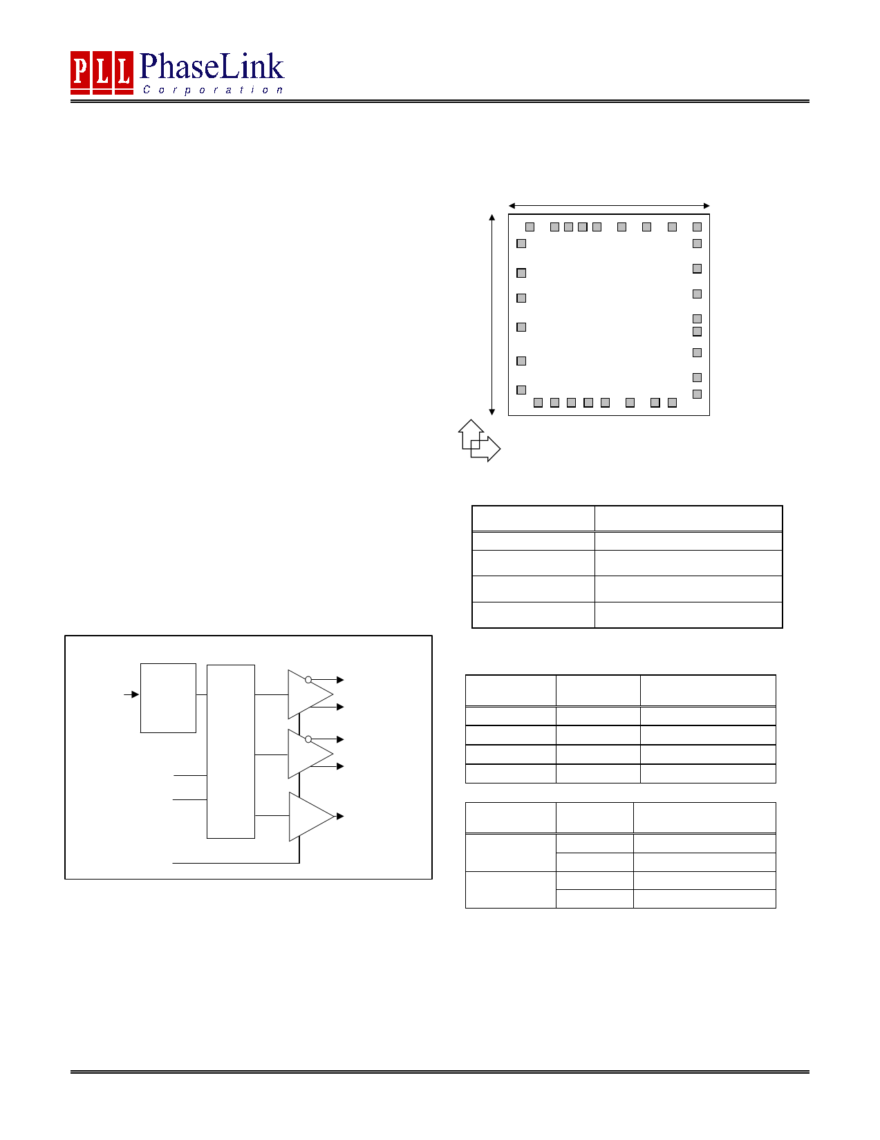
DIE CONFIGURATION
65 mil
25 24 23 22 21 20 19 18
26
(1550,1475)
17
16
15
27
14
28
13
29 12
11
30
10
31 9
12345 6 78
Y (0,0)
X
DIE SPECIFICATIONS
Name
Size
Reverse side
Pad dimensions
Thickness
Value
62 x 65 mil
GND
80 micron x 80 micron
10 mil
OUTPUT SELECTION AND ENABLE
Pad #18
OUTSEL1
0
0
1
1
Pad #25
OUTSEL0
0
1
0
1
Selected Output
High Drive CMOS
Standard CMOS
PECL
LVDS
OE_SELECT OE_CTRL
(Pad #9)
(Pad #30)
State
0 0 (Default) Output enabled
1 Tri-state
1 (Default)
0 Tri-state
1 (Default) Output enabled
Pad #9: Bond to GND to set to “0”, bond to VDD to set to “1”
Pad #30: Logical states defined by PECL levels if OE_SELECT (pad #9) is “0”
Logical states defined by CMOS levels if OE_SELECT is “1”
2880 Zanker Road, San Jose, CA 95134 Tel (408) 571-1668 Fax (408) 571-1688 www.phaselink.com Rev 8/10/10 Page 1
1 page 
(Preliminary) PL130-00
Selectable High Speed Translator Buffer to CMOS, PECL, LVDS
8. PECL Electrical Characteristics
PARAMETERS
Output High Voltage
Output Low Voltage
SYMBOL
VOH
VOL
CONDITIONS
RL = 50 to (VDD – 2V)
(see figure)
9. PECL Switching Characteristics
PARAMETERS
Clock Rise Time
Clock Fall Time
Output Clock Duty Cycle
SYMBOL
tr
tf
CONDITIONS
@20/80% - PECL
@80/20% - PECL
@ Vdd – 1.3V
MIN.
VDD – 1.025
MAX.
VDD – 1.620
MIN. TYP. MAX.
0.6 1.5
0.5 1.5
45 50 55
UNITS
V
V
UNITS
ns
ns
%
PECL Levels Test Circuit
OUT
VDD
50 2.0V
PECL Output Skew
OUT
50%
OUT
50
OUT
80%
50%
20%
OUT
tR
OUT
tSKEW
PECL Transistion Time Waveform
DUTY CYCLE
45 - 55%
55 - 45%
tF
2880 Zanker Road, San Jose, CA 95134 Tel (408) 571-1668 Fax (408) 571-1688 www.phaselink.com Rev 8/10/10 Page 5
5 Page | ||
| Páginas | Total 7 Páginas | |
| PDF Descargar | [ Datasheet PL130-00.PDF ] | |
Hoja de datos destacado
| Número de pieza | Descripción | Fabricantes |
| PL130-00 | Selectable High Speed Translator Buffer to CMOS | PhaseLink |
| PL130-05 | High Speed Translator Buffer to PECL | Micrel |
| PL130-07 | High Speed Translator Buffer to LVCMOS | Microchip |
| PL130-09 | High Speed Translator Buffer to LVDS | Micrel |
| Número de pieza | Descripción | Fabricantes |
| SLA6805M | High Voltage 3 phase Motor Driver IC. |
Sanken |
| SDC1742 | 12- and 14-Bit Hybrid Synchro / Resolver-to-Digital Converters. |
Analog Devices |
|
DataSheet.es es una pagina web que funciona como un repositorio de manuales o hoja de datos de muchos de los productos más populares, |
| DataSheet.es | 2020 | Privacy Policy | Contacto | Buscar |