|
|
|
PDF AS29F010 Data sheet ( Hoja de datos )
| Número de pieza | AS29F010 | |
| Descripción | 128K x 8 FLASH | |
| Fabricantes | Micross | |
| Logotipo | ||
Hay una vista previa y un enlace de descarga de AS29F010 (archivo pdf) en la parte inferior de esta página. Total 26 Páginas | ||
|
No Preview Available !
FLASH
AS29F010
128K x 8 FLASH
UNIFORM SECTOR 5.0V FLASH MEMO-
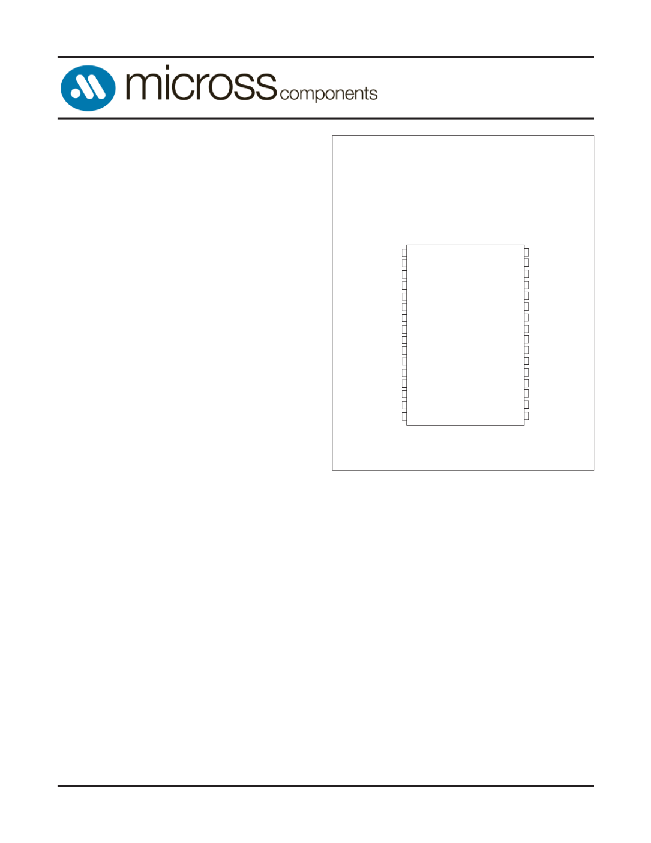
PIN ASSIGNMENT
(Top View)
AVAILABLE AS MILITARY
SPECIFICATIONS
• MIL-STD-883
• SMD 5962-96690
FEATURES
• Single 5.0V ±10% power supply operation
• Low power consumption:
3 12 mA typical active read current
3 30 mA typical program/erase current
3 <1 μA typical standby current
• Flexible sector architecture
3 Eight 16Kbyte sectors
3 Any combination of sectors can be erased
3 Full chip erase
• Sector protection
3 Hardware-based feature that disables/reenables program
and erase operations in any combination of sectors
3 Sector protection/unprotection can be implemented
using standard PROM programming equipment
• Embedded Algorithms
3 Embedded Erase algorithm automatically pre-programs
and erases the chip or any combination of designated
sectors
3 Embedded Program algorithm automatically programs
and verifies data at specified address
• Erase Suspend/Resume
3 Supports reading data from a sector not being erased
• Minimum 1,000,000 Program/Erase Cycles per sector
guaranteed
• Compatible with JEDEC standards
3 Pinout and software compatible with single-power-
supply FLASH
3 Superior inadvertent write protection
• Data\ Polling and Toggle Bits
3 Provides a software method of detecting program or
erase cycle completion
32-PIN Ceramic DIP (CW)
32-pin Flatpack (F)
32-pin Lead Formed Flatpack (DCG)
NC 1
A16 2
A15 3
A12 4
A7 5
A6 6
A5 7
A4 8
A3 9
A2 10
A1 11
A0 12
DQ0 13
DQ1 14
DQ2 15
VSS 16
32
31
VWCEC\
30 NC
29 A14
28 A13
27 A8
26 A9
25 A11
24 OE\
23 A10
22 CE\
21 DQ7
20 DQ6
19 DQ5
18 DQ4
17 DQ3
OPTIONS
• Timing
50ns
60ns
70ns
90ns
120ns
150ns
• Package
Ceramic DIP (600 mil)
Flatpack
Lead Formed Flatpack
Small Outline J-Lead
MARKING
-50
-60
-70
-90
-120
-150
CW
F
DCG
SOJ
For more products and information
please visit our web site at
www.micross.com
• Temperature
Industrial Temperature (-40°C to +85°C)
Military Temperature (-55°C to +125°C)
883C Processing (-55°C to +125°C)
QML Processing (-55°C to +125°C)
IT
XT
883C
Q
AS29F010
Rev. 2.6 11/10
Micross Components reserves the right to change products or specifications without notice.
1
1 page 
FLASH
AS29F010
Standby Mode
When the system is not reading or writing to the device, it
can place the device in the standby mode. In this mode, current
consumption is greatly reduced, and the outputs are placed in
the high impedance state, independent of the OE\ input.
The device enters the CMOS standby mode when the CE\
pin is held at VCC ± 0.5V. (Note that this is a more restricted
vmoolrtaegwehreanngCeEt\hiasnheVldIHa.)t
The device enters the TTL standby
VIH. The device requires the standard
access
If
ttihmeed(etCvEic)ebeisfodreesiet liescrteeaddydutorinregaderdaastuar.e
or
program-
ming, the device draws active current until the operation is
completed.
curreInCtC3spinecthifiecDatCioCn.haracteristics table represents the standby
Output Disable Mode
When the
disabled. The
OE\ input is at
output pins are
VpIlHac, eodutipnutthferohmightheimdpeevdicaencies
state.
Tables. The Command Definitions table shows the remaining
address bits that are don’t care. When all necessary bits have
been set as required, the programming equipment may then
read the corresponding identifier code on DQ7 - DQ0
To access the autoselect codes in-system, the host system
can issue the autoselect command via the command register, as
shown in the Command Definitions table. This method does
unsoitnrgeqthueiraeuVtoIsDe.lecSteme o“Cdeo.mmand Definitions” for details on
Sector Protection/Unprotection
The hardware sector protection feature disables both
program and erase operations in any sector. The hardware
sector unprotection feature re-enables both program and erase
operations in previously protected sectors.
Sector protection/unprotection must be implemented us-
ing programming equipment. The procedure requires a high
vdeovltiacgeeis(VshIDip) poend
address
with all
pin A9
sectors
and the control
unprotected. It
pins. The
is possible
to determine whether a sector is protected or unprotected. See
“Autoselect Mode” for details.
Autoselect Mode
The autoselect mode provides manufacturer and device
identification, and sector protection verification, through
identifier codes output on DQ7 - DQ0. This mode is primarily
intended for programming equipment to automatically match a
device to be programmed with its corresponding programming
algorithm. However, the autoselect codes can also be accessed
in-system through the command register.
When using programming equipment, the autoselect mode
requires
A0 must
VbeIDaos nshaodwdrnesins
pin
the
A9. Address pins A6, A1, and
Autoselect Codes (High Voltage
Method) table. In addition, when verifying sector protection,
the sector address must appear on the appropriate highest
order address bits. Refer to the corresponding Sector Address
Hardware Data Protection
The command sequence requirement of unlock cycles
for programming or erasing provides data protection against
inadvertent writes (refer to the Command Definitions table).
In addition, the following hardware data protection measures
prevent accidental erasure or programming, which might
otherwise be caused by spurious system level signals during
VnoCiCsep. ower-up and power-down transitions, or from system
Low VCC Write Inhibit
When VCC is less than VLKO, the device does not accept
any write cycles. This protects data during VCC power-up and
TABLE 2: SECTOR ADDRESSES TABLE
SECTOR
A16
A15
A14 ADDRESS RANGE
SA0
0 0 0 00000h - 03FFFh
SA1
0 0 1 04000h - 07FFFh
SA2
0 1 0 08000h - 0BFFFh
SA3
0 1 1 0C000h - 0FFFFh
SA4
1 0 0 10000h - 13FFFh
SA5
1 0 1 14000h - 17FFFh
SA6
1 1 0 18000h - 1BFFFh
SA7
1 1 1 1C000h - 1FFFFh
NOTE: All sectors are 16 Kbytes in size.
AS29F010
Rev. 2.6 11/10
Micross Components reserves the right to change products or specifications without notice.
5
5 Page 
FLASH
AS29F010
approximately 100μs, then returns to reading array data. If
not all selected sectors are protected, the Embedded Erase
algorithm erases the unprotected sectors, and ignores the
selected sectors that are protected.
If a program address falls within a protected sector, DQ6
toggles for approximately 2μs after the program command
sequence is written, then returns to reading array data.
The Write Operation Status table shows the outputs for
Toggle Bit I on DQ6. Refer to Figure 4 for the toggle bit
algorithm, and to the Toggle Bit Timings figure in the “AC
Characteristics” section for the timing diagram.
the operation has exceeded the timing limits, DQ5 produces a
“1.”
Under both these conditions, the system must issue the
reset command to return the device to reading array data.
DQ3: Sector Erase Timer
FIGURE 4: TOGGLE BIT ALGORITHM
Reading Toggle Bit DQ6
Refer to Figure 4 for the following discussion. Whenever
the system initially begins reading toggle bit status, it must
read DQ7-DQ0 at least twice in a row to determine whether a
toggle bit is toggling. Typically, a system would note and store
the value of the toggle bit after the first read. After the second
read, the system would compare the new value of the toggle
bit with the first. If the toggle bit is not toggling, the device
has completed the program or erase operation. The system can
read array data on DQ7-DQ0 on the following read cycle.
However, if after the initial two read cycles, the system
determines that the toggle bit is still toggling, the system also
should note whether the value of DQ5 is high (see the section on
DQ5). If it is, the system should then determine again whether
the toggle bit is toggling, since the toggle bit may have stopped
toggling just as DQ5 went high. If the toggle bit is no longer
toggling, the device has successfully completed the program
or erase operation. If it is still toggling, the device did not
complete the operation successfully, and the system must write
the reset command to return to reading array data.
The remaining scenario is that the system initially
determines that the toggle bit it toggling and DQ5 has not gone
high. The system may continue to monitor the toggle bit and
DQ5 through successive read cycles, determining the status
as described in the previous paragraph. Alternatively, it may
choose to perform other system tasks. In this case, the system
must start at the beginning of the algorithm when it returns to
determine the status of the operation (top of Figure 4).
DQ5: Exceeded Timing Limits
DQ5 indicates whether the program or erase time has
exceeded a specified internal pulse count limit. Under these
conditions DQ5 produces a “1.” This is a failure condition
that indicates the program or erase cycle was not successfully
completed.
The DQ5 failure condition may appear if the system tries
to program a “1” to a location that is previously programmed
to “0.” Only an erase operation can change a “0” back to a “1.”
Under this condition, the device halts the operation, and when
NOTE:
1) Read toggle bit twice to determine whether or not it is toggling. See text.
2) Recheck toggle bit because it may stop toggling as DQ5 changes to “1”.
See text.
AS29F010
Rev. 2.6 11/10
11
Micross Components reserves the right to change products or specifications without notice.
11 Page | ||
| Páginas | Total 26 Páginas | |
| PDF Descargar | [ Datasheet AS29F010.PDF ] | |
Hoja de datos destacado
| Número de pieza | Descripción | Fabricantes |
| AS29F010 | 5V 128K x 8 CMOS FLASH EEPROM | Alliance Semiconductor |
| AS29F010 | 128K x 8 FLASH | Micross |
| AS29F010 | 128K x 8 FLASH | Austin Semiconductor |
| Número de pieza | Descripción | Fabricantes |
| SLA6805M | High Voltage 3 phase Motor Driver IC. |
Sanken |
| SDC1742 | 12- and 14-Bit Hybrid Synchro / Resolver-to-Digital Converters. |
Analog Devices |
|
DataSheet.es es una pagina web que funciona como un repositorio de manuales o hoja de datos de muchos de los productos más populares, |
| DataSheet.es | 2020 | Privacy Policy | Contacto | Buscar |