|
|
|
PDF AS5SS256K18 Data sheet ( Hoja de datos )
| Número de pieza | AS5SS256K18 | |
| Descripción | 256K x 18 SSRAM | |
| Fabricantes | Micross | |
| Logotipo | ||
Hay una vista previa y un enlace de descarga de AS5SS256K18 (archivo pdf) en la parte inferior de esta página. Total 14 Páginas | ||
|
No Preview Available !
SSRAM
AS5SS256K18
256K x 18 SSRAM
Synchronous Burst SRAM,
Flow-Through
FEATURES
• Fast access times: 8, 10, and 15ns
• Fast clock speed: 113, 100, and 66 MHz
• Fast clock and OE\ access times
•
•
SSNinOglOe Z+E3.3MVO±D5E%foprorwedeur cseudp-pployw(VerDsDt)andby
• Common data inputs and data outputs
• Individual BYTE WRTIE control and GLOBAL WRITE
• Three chip enables for simple depth expansion and address
pipelining
• Clock-controlled and registered addresses, data I/Os and
control signals
• Interally self-timed WRITE cycle
• Burst control pin (interleaved or linear burst)
• Automatic power-down
• Low capacitive bus loading
• Available in Industrial, Enhanced, and Mil-Temperature
Operating Ranges
• RoHs compliant options available
OPTIONS
• Timing
7.5ns/8ns/113 MHz
8.5ns/10ns/100 MHz
10ns/15ns/66 MHz
MARKING
-8
-9
-10
• Packages
TQFP
DQ No. 1001
• Operating Temperature Ranges:
- Military -55oC to +125oC
- Enhanced -45oC to +105oC
- Industrial -45oC to +85oC
/IT
/ET
/XT
GENERAL DESCRIPTION
The Micross Components Synchronous Burst SRAM family
employs high-speed, low power CMOS designs that are fabricated
using an advanced CMOS process.
The 4Mb Synchronous Burst SRAMs integrate a 256K x 18, SRAM
core with advanced synchronous peripheral circuitry and a 2-bit burst
counter. All synchronous inputs pass through registers controlled by
a positive-edge-triggered single clock input (CLK). The synchronous
inputs include all addresses, all data inputs, active LOW chip enable
(CE\), two additional chip enables for easy depth expansion (CE2\,
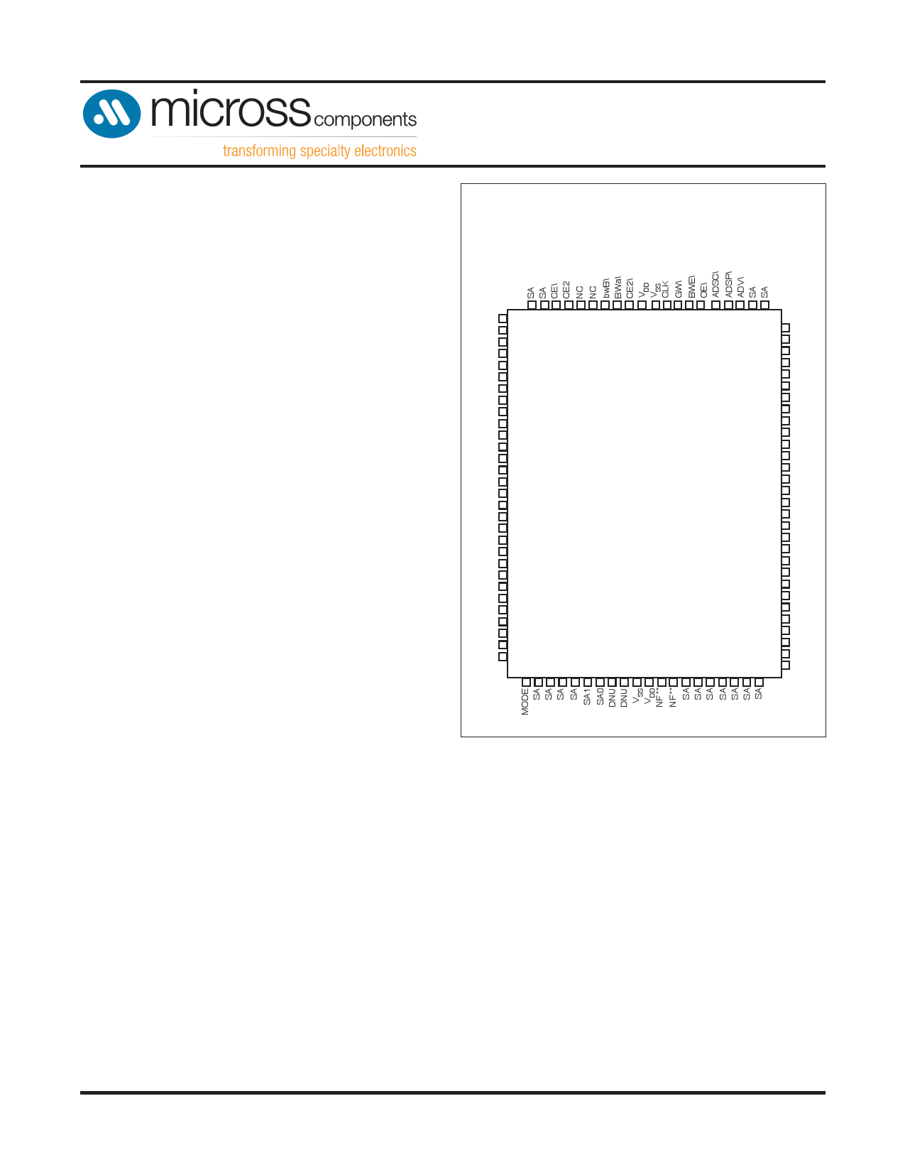
PIN ASSIGNMENT
(Top View)
100-pin TQFP (DQ)
NC
NC
NC
VDDQ
VSS
NC
NC
DQb
DQb
VSS
VDDQ
DQb
DQb
NC
VNDCD
DVQSbS
DQb
VDDQ
VSS
DQb
DQb
DQPb
NC
VSS
VDDQ
NC
NC
NC
1 100 99 98 97 96 95 94 93 92 91 90 89 88 87 86 85 84 83 82 81
2 80 SA
3 79 NC
4 78 NC
5 77 VDDQ
6 76 VSS
7 75 NC
8 74 DQPa
9 73 DQa
10 72 DQa
11 71 VSS
12 70 VDDQ
13 69 DQa
14 68 DQa
15
16
67
66
VNSCS
17
18
65
64
VZZDD
19 63 DQa
20 62 DQa
21 61 VDDQ
22 60 VSS
23 59 DQa
24 58 DQa
25 57 NC
26 56 NC
27 55
28 54
29 53
30 52
31 32 33 34 35 36 37 38 39 40 41 42 43 44 4546 47 48 49 50 51
VSS
VDDQ
NC
NC
NC
**pins 42,43 reserved for future address expansion for 8Mb, 16Mb densities.
CE2), burst control inputs (ADSC\, ADSP\, ADV\), byte write enables
(BWx\) and global write (GW\).
Asynchronous inputs include the output enable (OE\), clock (CLK)
and snooze enable (ZZ). There is also a burst mode input (MODE)
that selects between interleaved and linear burst modes. The data-out
(Q), enabled by OE\, is also asynchronous. WRITE cycles can be from
one to two bytes wide, as controlled by the write control inputs.
Burst operation can be initiated with either address status processor
(ADSP\) or address status controller (ADSC\) inputs. Subsequent
burst addresses can be internally generated as controlled by the burst
advance input (ADV\).
Address and write control are registered on-chip to simplify WRITE
cycles. This allows self-timed WRITE cycles. Individual byte enables
allow individual bytes to be written. During WRITE cycles on this
x18 device BWa\ controls DQa pins and DQPa; BWb\ controls DQb
pins and DQPb. GW\ LOW causes all bytes to be written. Parity bits
are available on this device.
The
power
4Mb Synchronous Burst SRAMs
supply, and all inputs and outputs
operate from a +3.3V
are TTL-compatible.
VThDDe
device is ideally suited for 486, Pentium®, and PowerPC systems and
those systems that benefit from a wide synchronous data bus.
AS5SS256K18
Rev. 2.5 10/13
Micross Components reserves the right to change products or specifications without notice.
1
1 page 
SSRAM
AS5SS256K18
ABSOLUTE MAXIMUM RATINGS*
Voltage on VDD Supply Relative to VSS............-0.5V to +4.6V
Voltage on VDDQ Supply Relative to VSS.........-0.5V to +4.6V
Storage Temperature (plastic) .....................-55C to +125C
Max Junction Temperature**.......................................+150C
Short Circuit Output Current..........…...........................100mA
*Stresses greater than those listed under “Absolute Maximum Ratings”
may cause permanent damage to the device. This is a stress rating only
and functional operation of the device at these or any other conditions
above those indicated in the operational sections of this specification
is not implied. Exposure to absolute maximum rating conditions for
extended periods may affect reliability.
**Maximum junction temperature depends upon package type, cycle
time, loading, ambient temperature and airflow.
DC ELECTRICAL CHARACTERISTICS AND RECOMMENDED OPERATING CONDITIONS
(-55oC < TA < +125oC, -40oC < TA < +105oC and -40oC<TA<+85oC; VDD = +3.3V ± 5% unless otherwise noted)
DESCRIPTION
Input High (Logic 1) Voltage
Input Low (Logic 0) Voltage
Input Leakage Current
Output Leakage Current
Output High Voltage
Output Low Voltage
Supply Voltage
Isolated Output Buffer Supply
CONDITIONS
(0V<VIN<VDD)
Output(s) disabled;
0V<VIN<VDD
IOH = -4.0mA
IOL = 8.0 mA
SYMBOL
VIH
VIL
ILI
ILO
VOH
VOL
VDD
VDDQ
MIN
2.0
-0.3
-2
-2
2.4
--
3.135
3.135
MAX
VDD +0.3
0.8
2
2
--
0.5
3.465
3.465
UNITS
V
V
P$
P$
V
V
V
V
NOTES
1, 2
1, 2
3
1, 4
1, 4
1
1, 5
CAPACITANCE
DESCRIPTION
Control Input Capacitance
Input/Output Capacitance (DQ)
CONDITIONS
TA = 25°C; f = 1MHz;
VDD = 3.3V
SYM
CI
CO
MAX
6
8
UNITS
pF
pF
NOTES
6
6
THERMAL RESISTANCE
DESCRIPTION
Thermal Resistance
(Junction to Ambient)
Thermal Resistance
(Junction to Top of Case)
CONDITIONS
Test conditions follow standard test
methods and procedures for measuring
thermal impedance, per EIA/JESD51
SYM
TJA
TJC
DQ DQC
Package Package UNITS
30.32 35.25 °C/W
6.85
7.96
°C/W
NOTES
6
6
NOTES:
1. All voltages referenced to VSS (GND)
2. Overshoot: VIH < +4.6V for t < tKC/2 for I < 20mA
Undershoot: VIL > -0.7V for t < tKC/2 for I < 20mA
Power-up: VIH < +3.465V and VDD<3.135V for t < 200ms
3. MODE pin has an internal pull-up, and input leakage = ±10μA.
4. The load used for VOH, VOL testing is shown in Figure 2 for 3.3V I/O. AC load current is higher then the stated DC values.
5. VDDQ should never exceed VDD. VDD and VDDQ can be connected together, for 3.3V I/O operation only.
6. This parameter is sampled.
AS5SS256K18
Rev. 2.5 10/13
Micross Components reserves the right to change products or specifications without notice.
5
5 Page 
CLK
tADSS
ADSP\
ADSC\
ADDRESS A1
BWE\, GW\
BWa\ - BWb\
CE\
(Note 2)
ADV\
tADSH
tAS
A2
tAH
tCES
tCEH
tKC READ/WRITE TIMING6
tKL
tKH
A3
tWS
A4
tWH
SSRAM
AS5SS256K18
A5 A6
OE\
tDS tDH
D High-Z
tOEHZ
Q Q(A1) Q(A2)
D(A3)
tOELZ
tKQ
Q(A4)
(NOTE 1)
Q(A4+1) Q(A4+2)
Q(A4+3)
D(A5)
D(A6)
Back-to-Back READS
(NOTE 5)
SINGLE WRITE
BURST READ
Back-to-Back
WRITE’s
Don’t Care
Undefined
NOTE: 1. Q(A4) refers to output from address A4. Q(A4+1) refers to output from the next internal burst address following A4.
2. CE2\ and CE2 have timing identical to CE\. On this diagram, when CE\ is LOW, CE2\ is LOW and CE2 is HIGH. When CE\ is HIGH, CE2\ is HIGH and CE2 is LOW.
3. The data bus (Q) remains in High-Z following a WRITE cycle unless an ADSP\, ADSC\, or ADV\ cycle is performed.
4. GW\ is HIGH.
5. Back-to-back READs may be controlled by either ADSP\ or ADSC\.
6. Timing is shown assuming that the device was not enabled before entering into this sequence.
AS5SS256K18
Rev. 2.5 10/13
11
Micross Components reserves the right to change products or specifications without notice.
11 Page | ||
| Páginas | Total 14 Páginas | |
| PDF Descargar | [ Datasheet AS5SS256K18.PDF ] | |
Hoja de datos destacado
| Número de pieza | Descripción | Fabricantes |
| AS5SS256K18 | 256K x 18 SSRAM | Micross |
| AS5SS256K18 | 256K x 18 SSRAM Synchronous Burst SRAM | Austin Semiconductor |
| Número de pieza | Descripción | Fabricantes |
| SLA6805M | High Voltage 3 phase Motor Driver IC. |
Sanken |
| SDC1742 | 12- and 14-Bit Hybrid Synchro / Resolver-to-Digital Converters. |
Analog Devices |
|
DataSheet.es es una pagina web que funciona como un repositorio de manuales o hoja de datos de muchos de los productos más populares, |
| DataSheet.es | 2020 | Privacy Policy | Contacto | Buscar |