|
|
|
PDF LNK305G Data sheet ( Hoja de datos )
| Número de pieza | LNK305G | |
| Descripción | Energy-Efficient Off-Line Switcher IC | |
| Fabricantes | Power Integrations | |
| Logotipo | ||
Hay una vista previa y un enlace de descarga de LNK305G (archivo pdf) en la parte inferior de esta página. Total 18 Páginas | ||
|
No Preview Available !
LNK302/304-306
LinkSwitch™-TN Family
Lowest Component Count, Energy-Efficient
Off-Line Switcher IC
Product Highlights
Cost Effective Linear/Cap Dropper Replacement
• Lowest cost and component count buck converter solution
• Fully integrated auto-restart for short-circuit and open loop
fault protection – saves external component costs
• LNK302 uses a simplified controller without auto-restart for
very low system cost
• 66 kHz operation with accurate current limit – allows low cost
off-the-shelf 1 mH inductor for up to 120 mA output current
• Tight tolerances and negligible temperature variation
• High breakdown voltage of 700 V provides excellent input
surge withstand
• Frequency jittering dramatically reduces EMI (~10 dB)
• Minimizes EMI filter cost
• High thermal shutdown temperature (+135 °C minimum)
Much Higher Performance Over Discrete Buck and
Passive Solutions
• Supports buck, buck-boost and flyback topologies
• System level thermal overload, output short-circuit and open
control loop protection
• Excellent line and load regulation even with typical configuration
• High bandwidth provides fast turn-on with no overshoot
• Current limit operation rejects line ripple
• Universal input voltage range (85 VAC to 265 VAC)
• Built-in current limit and hysteretic thermal protection
• Higher efficiency than passive solutions
• Higher power factor than capacitor-fed solutions
• Entirely manufacturable in SMD
EcoSmart™– Extremely Energy Efficient
• Consumes typically only 50/80 mW in self-powered buck
topology at 115/230 VAC input with no-load (opto feedback)
• Consumes typically only 7/12 mW in flyback topology with
external bias at 115/230 VAC input with no-load
• Meets California Energy Commission (CEC), Energy Star, and
EU requirements
Applications
• Appliances and timers
• LED drivers and industrial controls
Description
LinkSwitch-TN is specifically designed to replace all linear and
capacitor-fed (cap dropper) non-isolated power supplies in the
under 360 mA output current range at equal system cost while
offering much higher performance and energy efficiency.
LinkSwitch-TN devices integrate a 700 V power MOSFET,
oscillator, simple On/Off control scheme, a high-voltage switched
current source, frequency jittering, cycle-by-cycle current limit
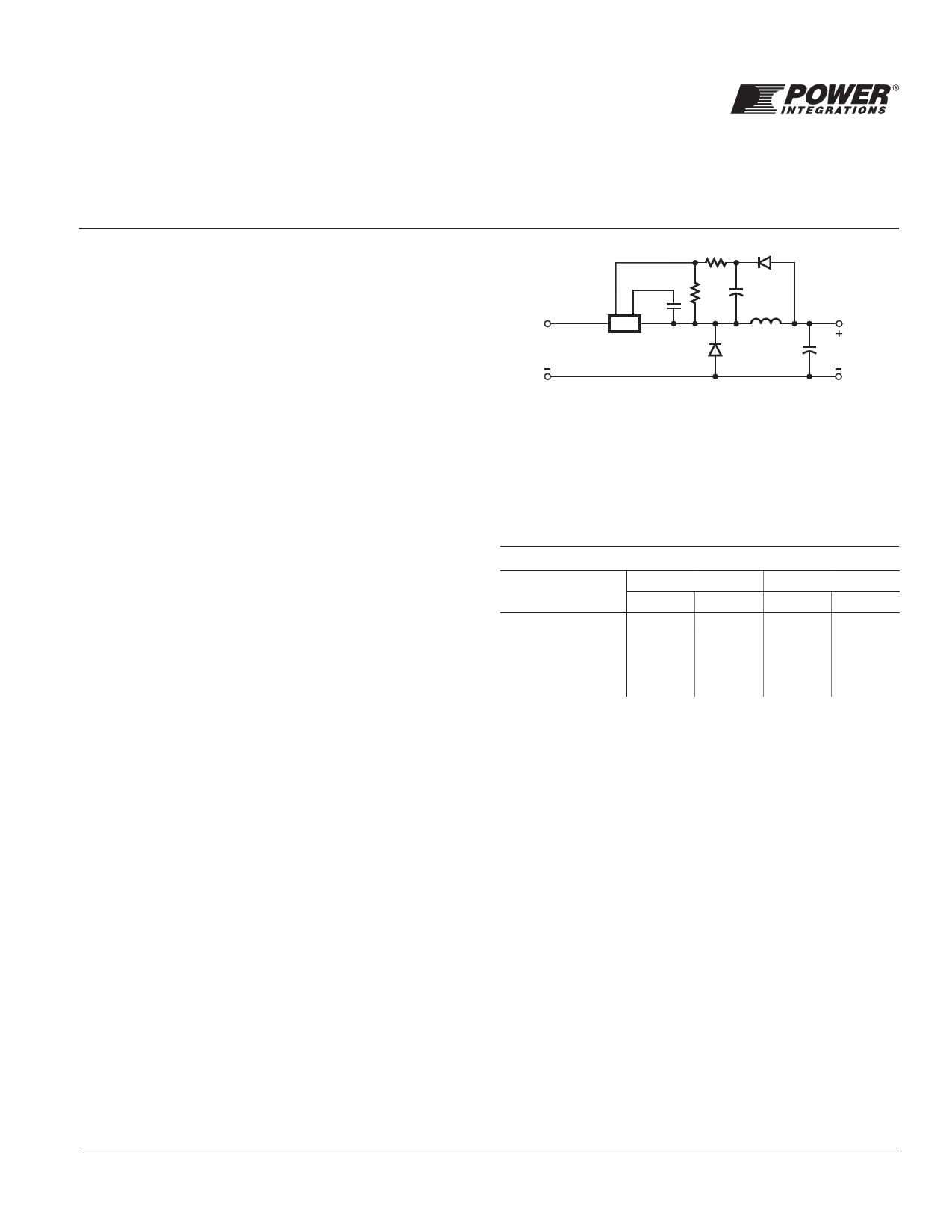
FB BP
Wide+Range
High-Voltage
DS
LinkSwitch-TN
DC Input
+
DC
Output
Figure 1.
PI-3492-041509
Typical Buck Converter Application (See Application Examples Section
for Other Circuit Configurations).
Output Current Table1
Product4
LNK302P/G/D
LNK304P/G/D
LNK305P/G/D
LNK306P/G/D
230 VAC ±15%
MDCM2
CCM3
63 mA
80 mA
120 mA 170 mA
175 mA 280 mA
225 mA 360 mA
85-265 VAC
MDCM2
CCM3
63 mA
80 mA
120 mA 170 mA
175 mA 280 mA
225 mA 360 mA
Table 1. Output Current Table.
Notes:
1. Typical output current in a non-isolated buck converter. Output power capability
depends on respective output voltage. See Key Applications Considerations
Section for complete description of assumptions, including fully discontinuous
conduction mode (DCM) operation.
2. Mostly discontinuous conduction mode.
3. Continuous conduction mode.
4. Packages: P: DIP-8B, G: SMD-8B, D: SO-8C.
and thermal shutdown circuitry onto a monolithic IC. The start-up
and operating power are derived directly from the voltage on the
DRAIN pin, eliminating the need for a bias supply and associated
circuitry in buck or flyback converters. The fully integrated
auto-restart circuit in the LNK304-306 safely limits output power
during fault conditions such as short-circuit or open loop,
reducing component count and system-level load protection
cost. A local supply provided by the IC allows use of a non-
safety graded optocoupler acting as a level shifter to further
enhance line and load regulation performance in buck and
buck-boost converters, if required.
www.powerint.com
This Product is Covered by Patents and/or Pending Patent Applications.
June 2013
1 page 
LNK302/304-306
AC
INPUT
RF1 D3
L2
C4 C5
D4
LinkSwitch-TN
D FB
R1
BP
S
S
C1
R3
C3
SS
D1
Optimize hatched copper areas (
) for heatsinking and EMI.
Figure 6a. Recommended Printed Circuit Layout for LinkSwitch-TN in a Buck Converter Configuration using P or G Package.
D2
+
L1
DC
OUTPUT
C2
PI-3750-041509
RF1 D3
L2
AC
INPUT
C4
D4
C5
DS
S L1
FB S
BP S D1
+
C1
C3
R3 R1
D2 C2
DC
OUTPUT
Optimize hatched copper areas (
) for heatsinking and EMI.
PI-4546-041509
Figure 6b. Recommended Printed Circuit Layout for LinkSwitch-TN in a Buck Converter Configuration using D Package to Bottom Side of the Board.
Key Application Considerations
LinkSwitch-TN Design Considerations
Output Current Table
Data sheet maximum output current table (Table 1) represents
the maximum practical continuous output current for both
mostly discontinuous conduction mode (MDCM) and continuous
conduction mode (CCM) of operation that can be delivered
from a given LinkSwitch-TN device under the following
assumed conditions:
1. Buck converter topology.
2. The minimum DC input voltage is ≥70 V. The value of input
capacitance should be large enough to meet this criterion.
3. For CCM operation a KRP* of 0.4.
4. Output voltage of 12 VDC.
5. Efficiency of 75%.
6. A catch/freewheeling diode with tRR ≤75 ns is used for MDCM
operation and for CCM operation, a diode with tRR ≤35 ns is
used.
7. The part is board mounted with SOURCE pins soldered to a
sufficient area of copper to keep the SOURCE pin tempera-
ture at or below 100 °C.
*KRP is the ratio of ripple to peak inductor current.
LinkSwitch-TN Selection and Selection Between
MDCM and CCM Operation
Select the LinkSwitch-TN device, freewheeling diode and
output inductor that gives the lowest overall cost. In general,
MDCM provides the lowest cost and highest efficiency converter.
CCM designs require a larger inductor and ultrafast (tRR ≤35 ns)
freewheeling diode in all cases. It is lower cost to use a larger
LinkSwitch-TN in MDCM than a smaller LinkSwitch-TN in CCM
because of the additional external component costs of a CCM
design. However, if the highest output current is required, CCM
should be employed following the guidelines below.
Topology Options
LinkSwitch-TN can be used in all common topologies, with or
without an optocoupler and reference to improve output voltage
tolerance and regulation. Table 2 provide a summary of these
configurations. For more information see the Application Note
– LinkSwitch-TN Design Guide.
www.powerint.com
5
Rev. J 06/13
5 Page 
LNK302/304-306
Parameter
Conditions
Symbol
SOURCE = 0 V; TJ = -40 to 125 °C
See Figure 7
Min
Typ
Max
Units
(Unless Otherwise Specified)
Output
ON-State
Resistance
OFF-State Drain
Leakage Current
RDS(ON)
IDSS
LNK302
ID = 13 mA
LNK304
ID = 25 mA
LNK305
ID = 35 mA
LNK306
ID = 45 mA
VBP = 6.2 V, VFB ≥2 V,
VDS = 560 V,
TJ = 25 °C
TJ = 25 °C
TJ = 100 °C
TJ = 25 °C
TJ = 100 °C
TJ = 25 °C
TJ = 100 °C
TJ = 25 °C
TJ = 100 °C
LNK302/304
LNK305
LNK306
48 55.2
76 88.4
24 27.6
38 44.2
12 13.8
W
19 22.1
7 8.1
11 12.9
50
70 mA
90
Breakdown Voltage
Rise Time
Fall Time
DRAIN Pin
Supply Voltage
Output Enable Delay
Output Disable
Setup Time
BVDSS
tR
tF
tEN
tDST
VBP
= 6.2
TJ =
V2,5V°FCB ≥2
V,
Measured in a Typical Buck
Converter Application
See Figure 9
700 V
50 ns
50 ns
50 V
10 ms
0.5 ms
Auto-Restart
ON-Time
tAR
STeJe=N2o5te°CH
LNK302
LNK304-306
Not Applicable
50
ms
Auto-Restart
Duty Cycle
DCAR
LNK302
LNK304-306
Not Applicable
6
%
Notes:
A.
Total current consumption is the
IS2 and IDSS when FEEDBACK pin
sisumshoofrtIeS1datnodSIODSUS RwCheEn(MFEOESDFBEATCsKwiptcinhivnogl)t.age
is
≥2
V
(MOSFET
not
switching)
and
the
sum
of
B. Since the output MOSFET is switching, it is difficult to isolate the switching current from the supply current at the DRAIN.
An alternative is to measure the BYPASS pin current at 6 V.
C. See Typical Performance Characteristics section Figure 14 for BYPASS pin start-up charging waveform.
D. This current is only intended to supply an optional optocoupler connected between the BYPASS and FEEDBACK
pins and not any other external circuitry.
E. For current limit at other di/dt values, refer to Figure 13.
F. This parameter is guaranteed by design.
G. This parameter is derived from characterization.
H. Auto-restart on time has the same temperature characteristics as the oscillator (inversely proportional to frequency).
www.powerint.com
11
Rev. J 06/13
11 Page | ||
| Páginas | Total 18 Páginas | |
| PDF Descargar | [ Datasheet LNK305G.PDF ] | |
Hoja de datos destacado
| Número de pieza | Descripción | Fabricantes |
| LNK305D | Energy-Efficient Off-Line Switcher IC | Power Integrations |
| LNK305G | Energy-Efficient Off-Line Switcher IC | Power Integrations |
| LNK305P | Energy-Efficient Off-Line Switcher IC | Power Integrations |
| Número de pieza | Descripción | Fabricantes |
| SLA6805M | High Voltage 3 phase Motor Driver IC. |
Sanken |
| SDC1742 | 12- and 14-Bit Hybrid Synchro / Resolver-to-Digital Converters. |
Analog Devices |
|
DataSheet.es es una pagina web que funciona como un repositorio de manuales o hoja de datos de muchos de los productos más populares, |
| DataSheet.es | 2020 | Privacy Policy | Contacto | Buscar |