|
|
|
PDF RT8121 Data sheet ( Hoja de datos )
| Número de pieza | RT8121 | |
| Descripción | Single Phase PWM Controller | |
| Fabricantes | Richtek | |
| Logotipo | ||
Hay una vista previa y un enlace de descarga de RT8121 (archivo pdf) en la parte inferior de esta página. Total 16 Páginas | ||
|
No Preview Available !
RT8121
Single Phase PWM Controller with 1-bit VID
General Description
RT8121 is a single phase PWM buck controller with one
integrated MOSFET driver for advanced microprocessor
application as VR12 VCCIO power. This controller
maintains the same features as the multi-phase product
family, but reduces the output to one phase for lower current
systems. Features of this controller include adjustable
operation frequency, power good indication, external error-
amp compensation, over voltage protection, over current
protection, externally adjustable offset voltage, load
transient enhancement (quick response), and enable/
shutdown control to achieve optimal power management
solution for various applications. The RT8121 comes in
the WQFN-20L 3x3 package.
Features
z Single Phase Power Conversion
z One Embedded MOSFET Driver with Internal
Bootstrap Diode
z 1-bit VID Table for VR12 VCCIO
z Continuous Differential Inductor DCR Current Sense
z Adjustable Soft-Start
z Adjustable Frequency Typically at 200kHz
z Power Good Indication
z Adjustable Over Current Protection
z Over Voltage Protection
z Over Temperature Protection
z Small 20-Lead WQFN Package
z RoHS Compliant and Halogen Free
Ordering Information
RT8121
Package Type
QW : WQFN-20L 3x3 (W-Type)
Lead Plating System
G : Green (Halogen Free and Pb Free)
Z : ECO (Ecological Element with
Halogen Free and Pb free)
Note :
Richtek products are :
RoHS compliant and compatible with the current require-
ments of IPC/JEDEC J-STD-020.
Suitable for use in SnPb or Pb-free soldering processes.
Marking Information
RT8121GQW
J1= : Product Code
J1=YM
DNN
YMDNN : Date Code
Applications
z VR12 VCCIO Voltage Regulator
z Low Voltage, High Current DC/DC Converter
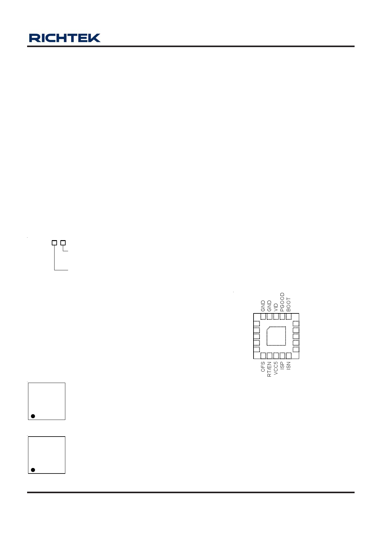
Pin Configurations
(TOP VIEW)
FBRTN
SS
COMP
FB
ADJ
20 19 18 17 16
1 15 UGATE
2 14 PHASE
3 GND 13 VCC12
4 21 12 LGATE
5 11 OCSET
6 7 8 9 10
WQFN-20L 3x3
RT8121ZQW
J1 YM
DNN
J1 : Product Code
YMDNN : Date Code
DS8121-02 May 2011
www.richtek.com
1
1 page 
RT8121
Parameter
Symbol
Test Conditions
RT/EN
Chip Disable Threshold
Running Frequency
RT Pin Voltage
VDIS
fOSC
VRT, GND
RT Pin Voltage
VRT, VDD
Modulation Gain
ARAMP
Reference Voltage Accuracy
DAC Accuracy
RRT = 60kΩ
RRT = 60kΩ, when RT
connected to GND by a register
RRT = 60kΩ, when RT
connected to VCC5 by a register
RRT = 60kΩ
VID Input Low Voltage
VID
VID Input High Voltage
VID
Error Amplifier
DC Gain
Gain-Bandwidth
Slew Rate
Output Voltage Range
Maximum Current
ADC
GBW
SR
VCOMP
IEA_SLEW
No Load
CLOAD = 10pF
CLOAD = 10pF
Slew
Power Sequence
PGOOD Low Voltage
Soft-Start Delay
VPGOOD IPGOOD = 4mA
TD1
PGOOD Delay
TD3
Current Sense Amplifier
Maximum Current
Input Offset Voltage
IGMMAX
VOSCS
VCSP = 1.3V, sink current from
CSN
Soft-Start
Soft-Start Current
VID Change Current
ISS1 Slew
ISS2 Slew
Gate Driver
UGATE Drive Source
UGATE Drive Sink
LGATE Drive Source
LGATE Drive Sink
IUGATEsr
RUGATEsk
ILGATEsr
RLGATEsk
VBOOT – VPHASE = 12V,
VUGATE – VPHASE = 6V
VBOOT – VPHASE = 12V,
VUGATE – VPHASE = 1V
VVCC12 = 12V, VLGATE = 6V
VVCC12 = 12V, VLGATE = 1V
Protection
Over Voltage Threshold
OCP Input Offset Voltage
Thermal Shutdown
VOVP
VOCOFS
Sweep FB Voltage, VFB − VEAP
Min
--
180
1.52
VVCC5 −
1.68
--
−0.5
--
0.8
--
--
10
0.5
300
--
0
0.05
100
−1.5
12
120
0.6
--
0.6
--
125
−10
--
Typ
--
200
1.6
VVCC5 −
1.6
22
--
--
--
80
10
--
--
--
--
--
--
--
0
16
160
1
1
1
0.8
150
--
160
Max
0.4
220
1.68
VVCC5 −
1.52
--
0.5
0.4
--
--
--
--
3.6
--
0.4
5
4
--
1.5
20
200
--
--
--
--
175
10
--
Unit
V
kHz
V
V
%/V
%
V
V
dB
MHz
V/μs
V
μA
V
ms
ms
μA
mV
μA
μA
A
Ω
A
Ω
mV
mV
°C
DS8121-02 May 2011
To be continued
www.richtek.com
5
5 Page 
RT8121
Output Voltage Differential Sensing
The RT8121 uses a high-gain low-offset error amplifier for
differential sensing. The CPU voltage is sensed between
the FB and FBRTN pins. A resistor (RFB) connects FB pin
with the positive remote sense pin of the CPU (VCCP),
while the FBRTN pin connects directly to the negative
remote sense pin of the CPU (VCCN). The error amplifier
compares VEAP = ( VDAC − VADJ) with the VFB to regulate
the output voltage.
No-Load Offset
In Figure 5, IOFSN and IOFSP are used to generate no-load
offset. Either IOFSN or IOFSP is active during normal
operation. Connect a resistor from OFS pin to GND to
activate IOFSN. IOFSN flows through RFB from the FB pin to
VCCP. In this case, a negative no-load offset voltage (VOFSN)
is generated.
VOFSN
= IOFSN ×RFB
=
0.8 ×RFB
ROFS
Connect a resistor from OFS pin to VCC5 to activate IOFSP.
IOFSP flows through RFB from VCCP to FB pin. In this case,
a positive no-load offset voltage (VOFSP) is generated.
VOFSP
= IOFSP ×RFB
=
6.4 ×RFB
ROFS
C2
CFB R1 C1
IOFSN
RFB
VCC_SNS
(Positive Remote
Sense Pin of CPU)
FB
IOFSP
VSS_SNS
(Negative Remote
Sense Pin of CPU)
+ +-
VDAC
-
+
EAP -
FBRTN
RADJ ADJ
COMP
Figure 5. Circuit for VOUT Differential Sensing and No-
Load Offset
Load Transient Quick Response
In steady state, the voltage of VFB is controlled to be very
close to VEAP. While a load step transient from light load
to heavy load could cause VFB to be lower than VEAP by
several tens of mV. In conventional buck converter design
(without non-linear control) for CPU VR application, due
to limited control bandwidth, it is hard for the VR to prevent
VOUT undershoot during quick load transient from light load
to heavy load. Hence, the RT8121 builds in a state-of-
the-art quick response function which detects load
transient by comparing VFB and VEAP. If VFB suddenly
drops below “VEAP−VQR”where VQR is a predetermined
voltage (~40mV), the quick response indicator QR rises
up. When QR = high, the RT8121 turns on all high side
MOSFETs and turns off all low side MOSFETs. The
sensitivity of quick response can be adjusted by varying
the values of CFB and RFB. Smaller RFB and/or larger CFB
will make QR easier to be triggered. Figure 6 is the circuit
and typical waveforms.
CFB C2
VOUT
RFB R1 C1
FB COMP
VEAP = VDAC - VADJ
-EA
+
QR Circuit
VIOOUUTT
QR
Figure 6. Load Transient Quick Response
Output Current Sensing
The RT8121 provides a low input offset Current Sense
Amplifier (CSA) to monitor the output current. The output
current of CSA (IX) is used for load line control and over
current protection. In this inductor current sensing
topology, RS and CS must be set according to the equation
below :
L
DCR
= RS × CS
DS8121-02 May 2011
www.richtek.com
11
11 Page | ||
| Páginas | Total 16 Páginas | |
| PDF Descargar | [ Datasheet RT8121.PDF ] | |
Hoja de datos destacado
| Número de pieza | Descripción | Fabricantes |
| RT8120 | Single-Phase Synchronous Buck PWM Controller | Richtek |
| RT8121 | Single Phase PWM Controller | Richtek |
| RT8127 | High Efficiency Dual-Channel Output Synchronous Buck PWM Controller | Richtek |
| Número de pieza | Descripción | Fabricantes |
| SLA6805M | High Voltage 3 phase Motor Driver IC. |
Sanken |
| SDC1742 | 12- and 14-Bit Hybrid Synchro / Resolver-to-Digital Converters. |
Analog Devices |
|
DataSheet.es es una pagina web que funciona como un repositorio de manuales o hoja de datos de muchos de los productos más populares, |
| DataSheet.es | 2020 | Privacy Policy | Contacto | Buscar |