|
|
|
PDF TMM41256AP-10 Data sheet ( Hoja de datos )
| Número de pieza | TMM41256AP-10 | |
| Descripción | N-channel dynamic RAM | |
| Fabricantes | Toshiba | |
| Logotipo | ||
Hay una vista previa y un enlace de descarga de TMM41256AP-10 (archivo pdf) en la parte inferior de esta página. Total 19 Páginas | ||
|
No Preview Available !
TOSHIBA MOS MEMORY PRODUCT
DESCRIPTION
TMM41256AP/AT/AZ-l0, TMM41256AP/AT/AZ-12
TMM41256AP/AT/AZ-15
The THH4l256AP/AT/AZ is the N-channel dynamic RAM organized 262,144 words by 1 bit.
Multiplexed address inputs permit the Ttill4l256AP/AT/AZ to be packaged in a standard 16
pin plastic DIP, 18 pin PLCC and 16 pin ZIP. The package size provides high system bit
densities and is compatible with 'videly available automated testing and insertion equip-
ment. The double layered HOS technology with polycide and poly Si permits the Uill4l256AP/
AT/A~ high speed operation. Also, the advanced circuit techniques have' realized low power
dissipation. System oriented features include single power supply of 5V±lO% tolerance,
direct interfacing capability with high performance logic families such. as schottky TTL.
In addition to the RAS only refresh mode, a CAS before p~s automatic refresh is available.
Another special feature of TMH4l256AP/AT/AZ is page mode, alloHing the user to access at
a high data rate.
FEATURES
• 262,144 words by I bit organization
• Fast access time and cycle time
THM41256AP/AT/AZ-lO/-12/-l5
p~S Access Time
lOOns/120ns/150ns
CAS Access Time
50ns/ 60ns/ 75ns
Cycle Time
190ns/220ns/260ns
• Single power supply of 5V±IO% with a built-
in VBB generator
• Low Pmver:
II/,Orot) MAX. Operating (Tf.il'141256AP/AT/AZ-lO)
385m\~ HAX. Operating (UfrI41256AP/AT/AZ-12)
3301'11'; MAX. Operating (THM41256AP/AT/AZ-15)
28mH HAX. Standby
• Output unlatched at cycle end allows
two-dimensional chip selection
• Common I/O capability using "EARLY
hTRITE" operation
• Read-Modify-Hrite, CAS before RAS
refresh, RAS-only refresh, Hidden
refresh, and Page Mode capability
• All inputs and output TTL compatible
• 256 refresh cycles/4ms
• Package
Plastic DIP
Tf.1H4l256AP
Plastic Leaded Chip Carrier: THM41256AT
Plastic ZIP
TH!141256AZ
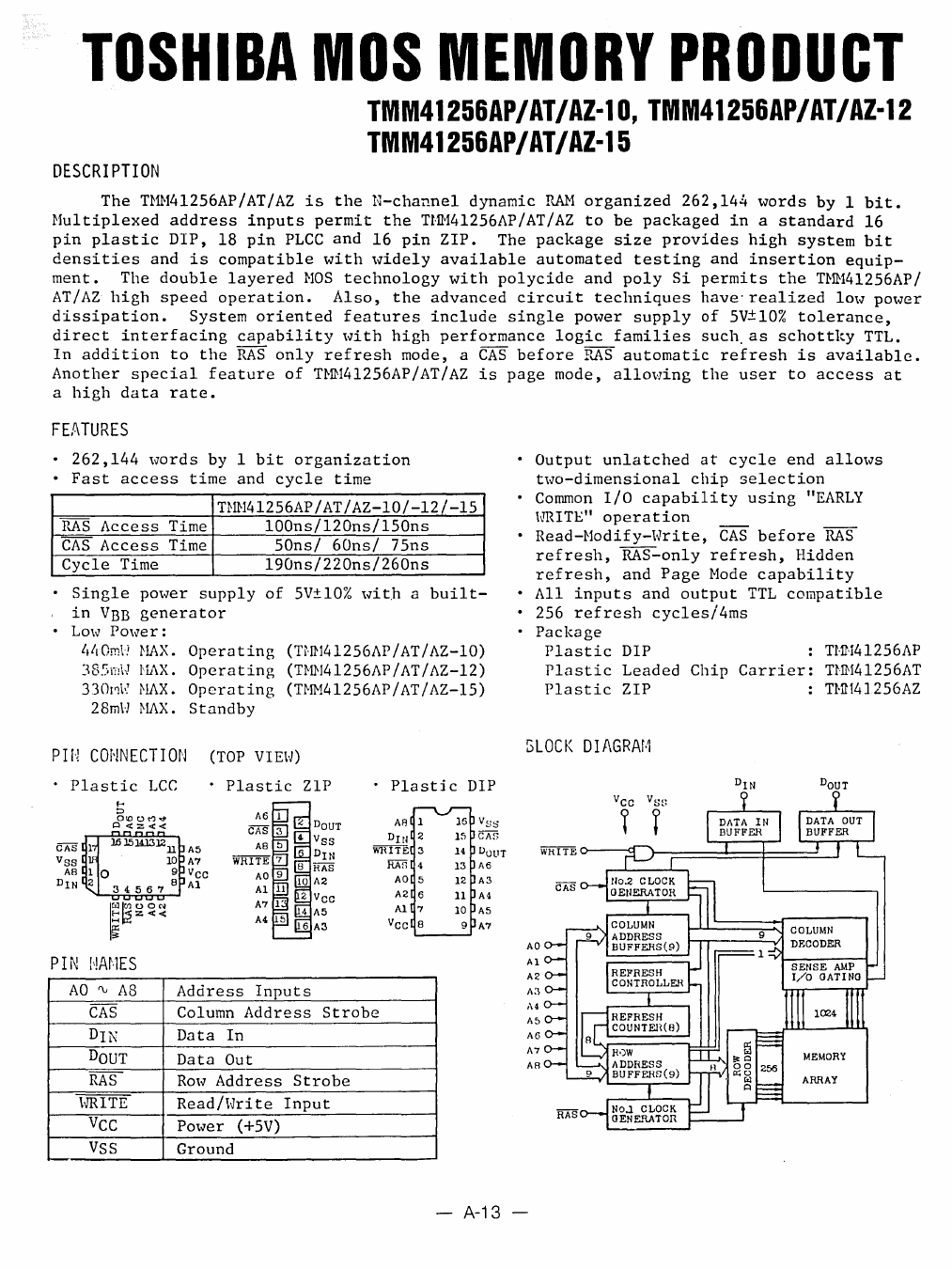
PIN CONNECTION (TOP VIEW)
· Plastic Lce . Plastic ZIP
SLOCK DIAGRAr·,
. Plastjc DIP
eAS 1
Vss
AS
DIN
PIN i'lAnES
AO 'V AS
CAS
DIN
DOUT
RAS
\VRITE
VCC
VSS
A5
A7
Vee
Al
All 1
DIU 2
WRITE 3
HAfl 4
AO 5
A2 6
Al 7
Vee 8
Address Inputs
Column Address Strobe
Data In
Data Out
Row Address Strobe
Read/Write Input
Pm.;rer (+5V)
Ground
16 Vs::;
15 CAfl
14 DOUT
13 A6
12 A3
11 A4
10 A5
AO
Al
A2
A:I
A4
A5
A6
A7
AS
- A-13 -
1 page 
TMM41256AP/AT/AZ-l0, TMM41256AP/AT/AZ-12
TMM41256AP/AT/AZ-15
NOTES:
1. Stresses greater than those listed under "Absolute Maximum Ratings" may cause
permanent damage to the device.
2. All voltages are referenced to Vss'
3. ICCl, ICC3, ICC4, ICCs depend on cycle rate.
4. ICCI, ICC4 depend on output loading. Specified values are obtained with the
output open.
5. An initial pause of 200~s is required after power-up followed by any 8 RAS
cycle~ before proper device operation is achieved. In case of using internal
refresh counter, a minimum of 8 CAS Before RAS initialization cycles instead
of 8 RAS cycles are required.
6. AC measurement assllme tT=sns.
7. VIH(min.) and VIL(max.) are reference levels for measuring timing of input
signals. Also, transition times are measured between VIH and VIL .
8. Assumes that tRCD ~ tRCD(max.). If tRCD is greater than the maximum recommended
value shown in this table, tRAC will increase by the amount that tRCD exceeds
the value shown.
9. Assume that tRCD ~ tRCD(max.)
10. Measured with a load equivalent to 2 TTL loads and 100pF.
11. tOFF(max.) defines the time at \v111CI1 tile output achieves the open circuit
condition and is not referenced to output voltage l~vcls.
]2. Either tRCH or tRRH must be satisfied for a read cycle.
13. Operation within the tRCD(max.) limit insures that tRAC(rr.ax.) can be met.
tRCD(max.) is specified as a reference point only: If tRCD is greater than the
specified tRCD(max.) limit, then access time is controlled exclusively by tCAC'
14. These parameters are referenced to CAS leading edge in early write cycles and
to WRITE leading edge in read-write or read-modify-write cycles.
15. tHCS' tC\.JD and tR\~D are not restrictive operating parameters. They are included
in the data sheet as electrical characteristics onl~1. If tHCS ~ t\~CS(min.),
the cycle is an early write cycle and the data out pin will remain open circuit
(high impedance) throughout the entire cycle; ] f tCHD ~ tCHD(·rr.in.) and tR\m ~ tRHD
(min.), the cycle is a read-write cycle or read-modify-write cycle and ~he data out
will contain ~ataread from the sele~ted cell: If neiiher of the above sets of
conditions is satisfied, the condition of the data out (at access time) is indeter-
minate.
- A-17 -
5 Page 
TMM41256AP/AT/AZ-l0, TMM41256AP/AT/AZ-12
TMM41256AP/AT/AZ-15
HIDDEN REFRESH CYCLE (READ)
AO-AB
\'IH -
VOH - - - - - - - - - - - < 1
vOL -
HIDDEN REFRESH CYCLE (HRITE)
~ Don't care
AO-AS
VIL -
DOUT
VOH
V~T
OPEN
- A-23 - -
~ Don't care
11 Page | ||
| Páginas | Total 19 Páginas | |
| PDF Descargar | [ Datasheet TMM41256AP-10.PDF ] | |
Hoja de datos destacado
| Número de pieza | Descripción | Fabricantes |
| TMM41256AP-10 | N-channel dynamic RAM | Toshiba |
| TMM41256AP-12 | N-channel dynamic RAM | Toshiba |
| TMM41256AP-15 | N-channel dynamic RAM | Toshiba |
| Número de pieza | Descripción | Fabricantes |
| SLA6805M | High Voltage 3 phase Motor Driver IC. |
Sanken |
| SDC1742 | 12- and 14-Bit Hybrid Synchro / Resolver-to-Digital Converters. |
Analog Devices |
|
DataSheet.es es una pagina web que funciona como un repositorio de manuales o hoja de datos de muchos de los productos más populares, |
| DataSheet.es | 2020 | Privacy Policy | Contacto | Buscar |