|
|
|
PDF CHY103 Data sheet ( Hoja de datos )
| Número de pieza | CHY103 | |
| Descripción | Charger Interface Physical Layer IC | |
| Fabricantes | Power Integrations | |
| Logotipo | ||
Hay una vista previa y un enlace de descarga de CHY103 (archivo pdf) en la parte inferior de esta página. Total 14 Páginas | ||
|
No Preview Available !
CHY103
ChiPhy™ Family
Charger Interface Physical Layer IC
with Complete System Level Protection
Product Highlights
• Supports Quick Charge 3.0 Class A and Class B specification
• Adaptive output overvoltage protection (AOVP)
• Secondary over-temperature protection (SOTP)
• Output soft short-circuit protection (OSSP)
• Remote shutdown protection (RESP)
• Enables Powered Device to shutdown adapter
• Selectable hysteretic or latching shutdown
• Power consumption below 1 mW at 5 V output
• Supports InnoSwitch™, TinySwitch™, and TOPSwitch™
Typical Applications
• Battery chargers for smart phones, tablets, netbooks,
digital cameras, and bluetooth accessories
• USB power output ports such as battery banks or car chargers
Description
CHY103 is a USB mobile device charger interface IC which implements
the Qualcomm’s Quick Charge 3.0 specification for adaptive voltage
battery charging. It incorporates all necessary functions to add Quick
Charge 3.0 capability to circuits incorporating Power Integrations’
switcher ICs such as InnoSwitch™, TinySwitch™, TOPSwitch™ and
other charger solutions employing traditional secondary-side feedback
schemes.
CHY103 supports the full output voltage range of Quick Charge 3.0,
including 200 mV micro-stepped voltage levels from 3.6 V to 12 V
(Class A) and up to 20 V (Class B). CHY103 provides a suite of system
level protection features protecting the power supply and connected
Powered Device (PD) from excessive output voltages, secondary-side
thermal overload, and faulty power delivery while adapter is unplugged.
Additionally it allows the PD to remotely shutdown the power supply
through USB data lines. The shutdown type can be configured as
either hysteretic or latching.
CHY103 automatically detects whether a connected PD is Quick Charge
3.0 or Quick Charge 2.0 capable before enabling output voltage
adjustment. If a PD that is not compliant to Quick Charge 2.0 or 3.0 is
detected, the CHY103 disables output voltage adjustment to ensure
safe operation with legacy 5 V only USB PDs.
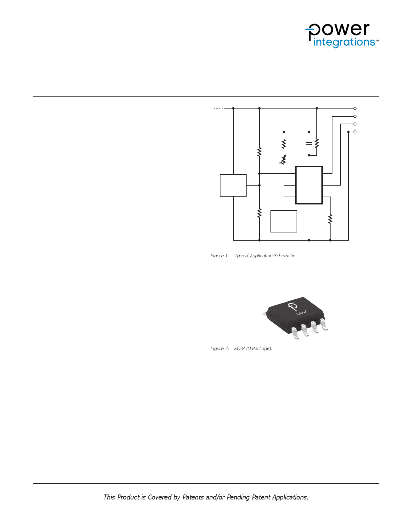
Voltage
Feedback
Network
FBD
BP
D+
TM
FA/P
CHY103
U1
D-
R
Fault
Handling
Circuit
GND
Figure 1. Typical Application Schematic.
PI-7612-091015
Figure 2. SO-8 (D Package).
VOUT
D+
D-
GND
www.power.com
This Product is Covered by Patents and/or Pending Patent Applications.
September 2015
1 page 
CHY103
through a 150 µA current source. This signal can for instance be
used to initiate hysteretic shutdown in a power supply employing
InnoSwitch through circuitry Q1, Q2, D1, and R3 as shown in Figure 5.
Alternatively a primary-side latching shutdown can be configured by
driving optocoupler U3 through Q1 and R5 as depicted in Figure 8.
The FA/P pin is clamped internally to 1 V during normal operation.
Adaptive Output Overvoltage Protection
CHY103 monitors the voltage present at the FEEDBACK DRIVE pin in
order to prevent excessive output voltage levels in case the power
supply control loop lost regulation. The OV comparator threshold
VTH(OV) (see Figure 6) is adapted to the set output voltage level (5 V,
9 V, 12 V, or 20 V) outside Quick Charge 3.0 continuous mode. As
soon as the output voltage reaches 120% of the set output voltage
CHY103 activates the protection mode if the OV fault is present for at
least 50 µs. Adaptive OVP is blanked for 500 ms when set output
voltage is stepped down outside of continuous mode (for instance
from 9 V to 5 V).
In Quick Charge 3.0 continuous mode the OV comparator threshold is
fixed to the respective maximum output voltage set by resistor RREF.
The resulting actual output OV level VOUT(OV) in continuous mode
depends on the respective voltage VOUT(SET) and is as follows:
VOUT^OVh = VOUT^SETh + 2.4 V
System Level Fault Protection
CHY103 offers an optional system level check to verify that power
delivered by the power supply is not caused by a possible soft-short
circuit present at the output but is requested by a connected PD. The
system fault check is either activated automatically by CHY103 when
no PD is connected (D+ is below 0.325 V) or can be initiated remotely
through the connected PD as outlined in the flowchart shown in Figure 9.
The FAULT MONITOR/PROTECTION pin monitors the switching
frequency of InnoSwitch through a voltage to frequency converter RFR
and CFR (refer to Figure 5). When the voltage at the FAULT MONITOR/
PROTECTION pin exceeds 0.325 V, a fault is flagged and CHY103
activates the protection mode if the fault is present for at least 40 ms.
The fault monitor input is only active when no PD is connected (D+ is
below 0.325 V) or a connected PD initiates a remote system level
TM
R4
STM
+
VTH(TM)
BP
ITM
tD(TM)
FA/P
Logic
-tO RNTC
PI-7695-081915
Figure 10. Optional Thermal Monitor Through NTC Resistor.
Start Remote
OSSP
Remote OSSP
Completed
Reduce Load
Current to <50 mA
Set D+ to High
Impedance
Initiate USB BC 1.2
and QC 3.0
Handshake
Yes
5 V Output
Present?
No
System Fault
Notification
CHY103 Detected
System Fault and
Shutdown Adapter
CHY103 Initiates
System Level Fault
Monitor
Figure 9. Remote System Level Check Flowchart.
www.power.com
Wait Minimum
40 ms
PI-7697-081915
5
Rev. D 09/15
5 Page 
CHY103
Parameter
Symbol
Conditions
SOURCE = 0 V; TJ = -20 °C to +85 °C
(Unless Otherwise Specified)
FEEDBACK Pin Drive Functions
Toggle Up Current
Source Step
∆IT(UP)
Toggle Down Current
Source Step
Protection Functions
∆IT(DO)
Output Overvoltage
Threshold
V TH(OV)
QC 2.0 Mode
Class A / Class B
QC 3.0
Continuous Mode
IT(UP) = 0 (5 V)
IT(UP) = 40 mA (9 V)
IT(UP) = 70 mA (12 V)
IT(UP) = 150 mA (20 V)
RREF = 38.3 kW
Class A
RREF = 12.4 kW
Class B
Output OV Detection
Delay Time
tD(OV)
Output OV Detection
Blanking Time
tB(OV)
Output Socket Fault
Detection Threshold
V TH(FA)
Socket Fault Detection
Delay Time
tD(FA)
FA/P Pin Clamp Voltage
Over-Temperature
Detection Threshold
VCL
V TH(TM)
ICLAMP = 100 mA
Over-Temperature
Detection Delay Time
tD(TM)
Temperature Monitor
Current Source
ITM
Temperature Monitor
Current On-Time
tON(ITM)
Temperature Monitor
Current Duty Ratio
DITM
Protection Mode
Current Source
IP
NOTES:
A. Guaranteed by design. Not tested in production.
Min
1.44
1.60
1.74
2.12
1.74
2.12
500
0.250
1.12
100
Typ
2
2
1.52
1.72
1.87
2.28
1.87
2.28
50
0.325
40
1
1.20
1
100
12
1
150
Max Units
mA
mA
1.60
1.84
2.00
2.44
2.00
2.44
0.400
1.28
200
V
ms
ms
V
ms
V
V
ms
mA
ms
%
mA
www.power.com
11
Rev. D 09/15
11 Page | ||
| Páginas | Total 14 Páginas | |
| PDF Descargar | [ Datasheet CHY103.PDF ] | |
Hoja de datos destacado
| Número de pieza | Descripción | Fabricantes |
| CHY100 | Charger Interface Physical Layer IC | Power Integrations |
| CHY103 | Charger Interface Physical Layer IC | Power Integrations |
| Número de pieza | Descripción | Fabricantes |
| SLA6805M | High Voltage 3 phase Motor Driver IC. |
Sanken |
| SDC1742 | 12- and 14-Bit Hybrid Synchro / Resolver-to-Digital Converters. |
Analog Devices |
|
DataSheet.es es una pagina web que funciona como un repositorio de manuales o hoja de datos de muchos de los productos más populares, |
| DataSheet.es | 2020 | Privacy Policy | Contacto | Buscar |