|
|
|
PDF MLX90132 Data sheet ( Hoja de datos )
| Número de pieza | MLX90132 | |
| Descripción | 13.56MHz RFID / NFC Transceiver | |
| Fabricantes | Melexis | |
| Logotipo | ||
Hay una vista previa y un enlace de descarga de MLX90132 (archivo pdf) en la parte inferior de esta página. Total 30 Páginas | ||
|
No Preview Available !
MLX90132
13.56MHz RFID / NFC Transceiver
Features and Benefits
Conforms with ISO/IEC 18092 (NFC)
Conforms with ISO/IEC 14443A and B,
Conforms with ISO/IEC 15693
Conforms with ISO/IEC 18000-3 mode 1
High speed communication (up to 848kbit/s)
Standard SPI/UART interfaces
Built-in Field and TAG detectors
Application Examples
NFC enabled car for access and start
Combo NFC and Wireless Power Charging
solutions
NFC applications in Industrial area (e.g. White
goods, security …)
Ordering Information
Part Code
MLX90132
MLX90132
Temperature Code
R (-40°C to 105°C)
R (-40°C to 105°C)
MLX90132
MLX90132
S (-20°C to 85°C)
S (-20°C to 85°C)
Package Code
Option Code
LQ (Lead free QFN 5x5 32 leads) AEA-000
LQ (Lead free QFN 5x5 32 leads) AEA-000
LQ (Lead free QFN 5x5 32 leads) AEA-000
LQ (Lead free QFN 5x5 32 leads) AEA-000
Packing Form Code
RE
TU
RE
TU
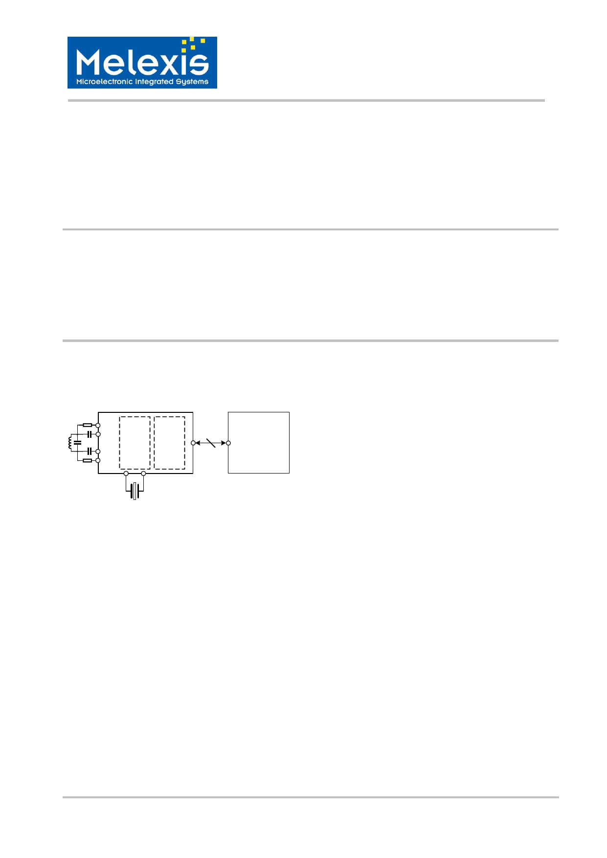
Functional Diagram
MLX90132
RX1
TX1
TX2 Analog Digital
RX2 section section
SPI/UART
microcontroller
Figure 1: MLX90132 functional diagram
Description
The MLX90132 is a 13.56MHz, fully integrated,
multi-protocol RFID/NFC transceiver IC. It has
been designed to handle sub-carrier frequencies
from 106 to 848 kHz and baud rates up to
848kbit/s.
The dual driver architecture of the MLX90132
requires minimal external support components
and allows the transmitter to provide up to
300milliwatts RF power to an appropriate antenna
load. This delivered power is suitable for most
short to mid-range applications.
The MLX90132 embeds tag emulation
functionality to support NFC Peer to Peer passive
communication mode. Enhanced tag and field
detection capabilities provide significant power
consumption reduction in RFID reader
configuration and in NFC mode.
The digital section of the MLX90132 handles the
low protocol layers from API to physical layer
using advanced bit and frame encoding/decoding
functions. It contains a digital demodulator based
on sub-carrier detection and a programmable
bit/symbol encoder/decoder. It also encodes and
decodes the start and stop bits, parity bits, extra
guard time (EGT), start and end of frame
(SOF/EOF) and CRC.
Its 528 byte buffer handles an entire RFID frame.
The SPI/UART communication ports guarantee
easy interface with the majority of
microcontrollers.
3901090132
Rev. 009
Page 1 of 44
Jan-2014
1 page 
MLX90132
13.56MHz RFID / NFC Transceiver
RX Reader
The reception stage of the MLX90132 is used in Reader mode to receive information from a transponder or
an NFC/RFID device. This stage performs the analog demodulation using two internal diode detectors on
RX1 and RX2.The information is then filtered with the appropriate bandwidth and finally digitized for further
processing. The receiver inputs RX1 and RX2 are typically connected to the resonance point of the antenna,
through two external attenuation resistors or capacitors to avoid saturation of the internal detector set to
VRXMAX. The complete receiver stage is automatically configured according to the protocol in use (Protocol
select command (0x02)).
Tag Front-end
This block is enabled in Tag emulation mode and performs all operations related to Tag emulation
functionality with low power consumption. The modulated information coming from an NFC/RFID device is
demodulated through the two built-in detectors connected on RX1 and RX2, filtered with the appropriate
bandwidth and finally digitized for further processing. The full settings of the Tag front-end stage are
automatically set with the selected protocol using the Protocol select command (0x02). The load modulation
used to send back the information in TAG emulation mode is also performed by the Tag front-end block. In
this case, an internal resistor is connected between the two inputs RX1 and RX2, modifying the antenna load.
Digital control & protocol handling
This block is responsible for the control of the device, as well as the frame coding and decoding parts of the
protocols supported by the MLX90132. The MLX90132 exchanges with the application microcontroller, pure
payload information after adding/removing frame related information such as SOF, EOF, EGT … It can also
be configured to calculate the CRC for each communication protocol.
Interface Block
The MLX90132 is addressed through SPI or UART (Reader mode only) interfaces with a specific and simple
set of commands. The built-in 528 byte buffer allows minimum interaction with the application microcontroller.
This reduces the burden of the microcontroller whose resources can be fully dedicated for the application.
Tag/Field Detector
This block manages the enhanced Tag and Field detection capabilities. It generates a detection signal that is
available for the application microcontroller through the interrupt pin IRQ_OUT. It allows the use of the
MLX90132 with low power consumption constraints.
Reference clock and internal oscillator
The built-in reference oscillator works with a reference crystal fXTAL of 27.12MHz from which the internal
nominal system clock frequency fHFO of 13.56 MHz is derived. An internal low frequency RC oscillator
frequency fLFO of 32 kHz is used for low-power operating modes, for example to control the internal timings.
In TAG emulation mode the clock is recovered from the HF field, through the built-in Clock Recovery block. In
case of field loss (e.g. during Reader modulation), an internal backup clock of ~10MHz is used instead.
Power management
The MLX90132 features 2 modes of operation (Active and Idle), subdivided in 6 different states of operation:
Hibernate, the device typically consumes 1µA
Sleep, the device typically consumes 20µA
TAG detection, the device typically consumes 45µA.
TAG emulation, the device typically consumes 2.5mA.
Ready (RF field OFF), the device typically consumes 2.5mA.
Reader, the consumption depends on the antenna load and on the operating conditions
3901090132
Rev. 009
Page 5 of 44
Jan-2014
5 Page 
MLX90132
13.56MHz RFID / NFC Transceiver
Reading data from the MLX90132
MOSI
Control byte
MISO
Several data bytes
Figure 8: SPI communication, reading data from the MLX90132
Data must be sampled by the rising edge of the SPI_SCK signal.
‘Sending’, ‘Polling’ and ‘Reading’ commands must be separated by a high level of the SPI_NSS line.
For example, when the application needs to wait for data from the MLX90132, it sets to low the pin SPI_NSS
and issues a ‘Polling’ command. By keeping the SPI_NSS “low”, the application can continuously read the
Flags waiting for the bit indicating that the MLX90132 is ready (the flags will be automatically updated, no
need to send several polling commands).Then, the application has to set high the pin SPI_NSS to finish the
polling sequence. The application puts low again the pin SPI_NSS to issue a ‘Reading’ command to read
data. When all data is read, the application sets high the pin SPI_NSS to terminate the communication.
The MLX90132 can issue as many 'Polling' commands as necessary.
For example, the application sets low the pin SPI_NSS to issue a 'Polling' commands. If the MLX90132 is not
ready, the application can put high the pin SPI_NSS and continue its operations. Then, as soon as the
application is ready again, it sets low the pin SPI_NSS to issue a 'Polling' commands, to see if the MLX90132
is ready. These operations are not time critical which makes it easy to insert in the application flow.
Reset MLX90132
MOSI
Control byte
MISO
Figure 9: SPI communication reset the MLX90132
Control byte 0x01 resets the MLX90132 and places the device in Power-up state. A wake-up sequence is
then necessary to start again the communication with the MLX90132.
Warning: The SPI communication is most significant bit (MSB) first.
5.2.2 IRQ mode
When the MLX90132 is configured to use the SPI serial interface, the pin IRQ_OUT is used to give additional
information to the application. When the MLX90132 is ready to send back a reply it sends an Interrupt
request by setting a low level on pin IRQ_OUT, which remains low until the application reads the data. The
application can use the IRQ mode to skip the polling stage.
3901090132
Rev. 009
Page 11 of 44
Jan-2014
11 Page | ||
| Páginas | Total 30 Páginas | |
| PDF Descargar | [ Datasheet MLX90132.PDF ] | |
Hoja de datos destacado
| Número de pieza | Descripción | Fabricantes |
| MLX90131 | 13.56MHz RFID / NFC Transceiver | Melexis |
| MLX90132 | 13.56MHz RFID / NFC Transceiver | Melexis |
| Número de pieza | Descripción | Fabricantes |
| SLA6805M | High Voltage 3 phase Motor Driver IC. |
Sanken |
| SDC1742 | 12- and 14-Bit Hybrid Synchro / Resolver-to-Digital Converters. |
Analog Devices |
|
DataSheet.es es una pagina web que funciona como un repositorio de manuales o hoja de datos de muchos de los productos más populares, |
| DataSheet.es | 2020 | Privacy Policy | Contacto | Buscar |