|
|
|
PDF MLX91207 Data sheet ( Hoja de datos )
| Número de pieza | MLX91207 | |
| Descripción | High Speed Hall Sensor IC | |
| Fabricantes | Melexis | |
| Logotipo | ||
Hay una vista previa y un enlace de descarga de MLX91207 (archivo pdf) en la parte inferior de esta página. Total 21 Páginas | ||
|
No Preview Available !
MLX91207
High Speed Hall Sensor IC
Features and Benefits
Programmable high speed Hall sensor
Wide bandwidth, short response time 8µs
Programmable linear transfer characteristic
Selectable analog ratiometric output
Measurement range from ±15mT to ±400mT
Thermometer output
17 bit ID number
Single die SOIC8 package RoHS compliant
Lead free component, suitable for lead free
soldering profile 260 °C
Low thermal Drift (Gain and Offset)
Application Examples
Current sensor applications
Over current detection circuit
Inverter Application HEV &EV
AC/DC converters
Battery management
Position sensor application
Ordering Code
Product Temperature Code Package Code
Ordering
Code
Option Code
MLX91207 L (-40°C to 150°C) DC (SOIC)
CAA-005
MLX91207 L (-40°C to 150°C) DC (SOIC)
CAA-005
MLX91207 L (-40°C to 150°C) DC (SOIC)
CAA-007
MLX91207 L (-40°C to 150°C)
MLX91207 L (-40°C to 150°C)
MLX91207 L (-40°C to 150°C)
DC (SOIC)
DC (SOIC)
DC (SOIC)
CAA-007
CAA-015(1)
CAA-015(1)
(1) Ratiometry is disabled by default for this version
Packing
form Code
TU (Tube)
RE (Reel)
TU
RE
TU
RE
Comment
15-45mV/mT (25mV/mT)
15-45mV/mT (25mV/mT)
5-20mV/mT (10mV/mT)
5-20mV/mT (10mV/mT)
15-45mV/mT (25mV/mT)
15-45mV/mT (25mV/mT)
Ordering example : MLX91207-LDC-CAA-007-TU
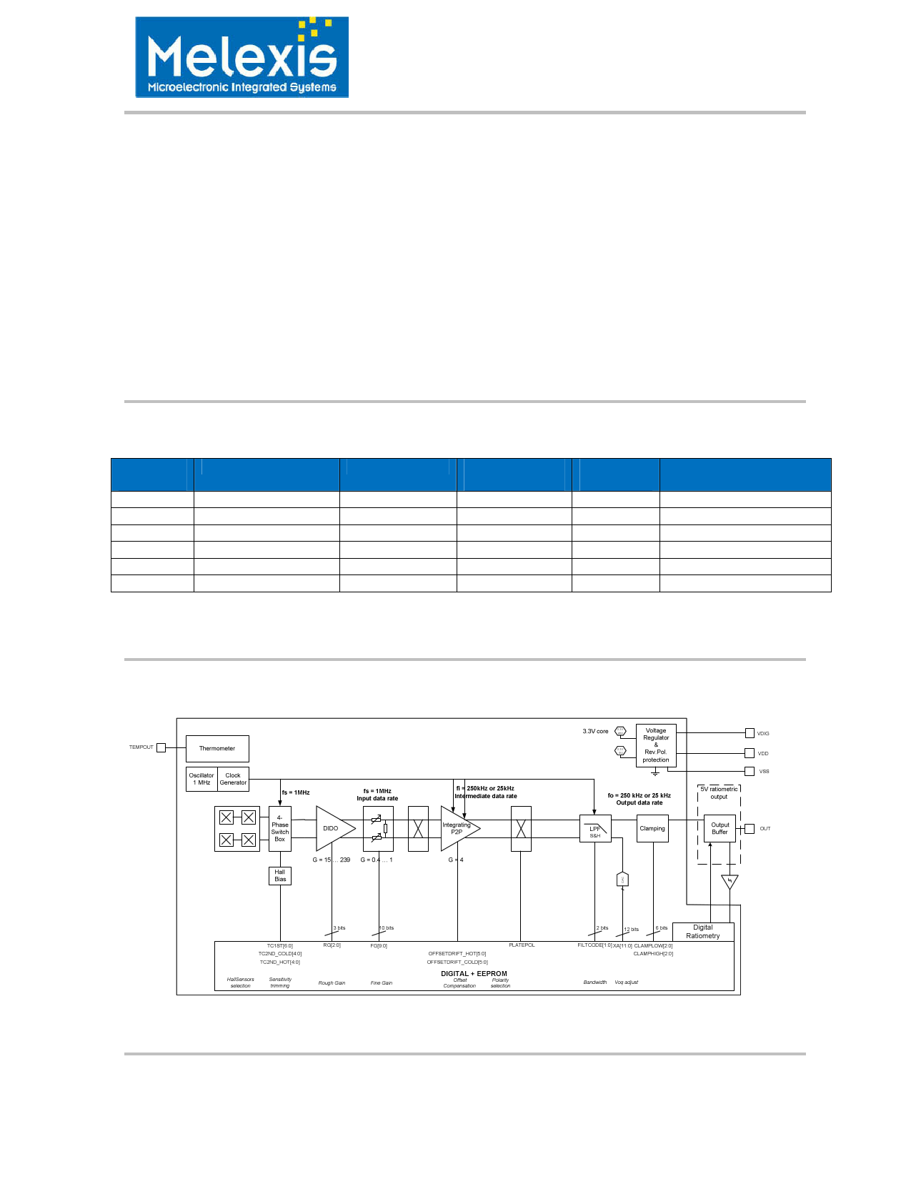
1 Functional Diagram
Figure 1: Block diagram
39010091207
Rev 17
Page 1 of 21
Data Sheet
April/12
1 page 
MLX91207
High Speed Hall Sensor IC
7 General Electrical Specifications
Operating Parameters TA = -40oC to 125oC, Vdd = 5.0 V, Iout = +/-2mA, recommended application diagram in
section 14 used, unless otherwise specified.
Parameter
Nominal Supply Voltage
Supply Current
Output Current
Output Resistance
Output Capacitive Load
Output Short Circuit Current
Leakage current
Output Voltage Swing (Linear
Range)
High-impedance mode levels(1)
BrokenVss Output Levels(1)
BrokenVdd Output Levels(1)
Under-voltage detection (1) (4)
Over-voltage detection mode1 (1) (4)
Over-voltage detection mode 2 (1) (4)
Clamped Output Level
Symbol Test Conditions
Vdd
Idd Without output load
TA = -40oC to 150oC
Iout
Vout = 50% Vdd, RL = 5kΩ
Cload
Ishort Output shorted to Vdd - Permanent
Output shorted to Vss - Permanent
Ileak High impedance mode (1)
Vout_pd
pull down ≥ 10 kΩ
Vout_pu
pull up ≥ 10 kΩ
Vout_HiZ_pu pull-up RL ≤ 30 kΩ
Vout_HiZ_pd pull-down RL ≤ 30 kΩ
OUT with pull-down RL ≤ 10 kΩ
OUT with pull-up RL ≤ 30 kΩ (2)
OUT with pull-down RL ≤ 30 kΩ (2)
OUT with pull-up RL ≤ 30 kΩ (2)
Vdd_uvd
Detected Voltage (L to H)
Vdd_uvh
Hysteresis
Vdd_ovd1
Detected Voltage (L to H)
Vdd_ovh1
Hysteresis
Vdd_ovd2
Detected Voltage (L to H)
Vdd_ovh2
Hysteresis
Clamp_lo Trimming Range
Clamp_hi Trimming Range
Min
4.5
-2
5
5
5
97
97
97
3.15
0.25
7.9
0.8
6.7
0.05
5 (3)
90
Typ Max
5 5.5
9 12
2
15
10 50
Not Destroyed
Not Destroyed
5
95
95
3
3
3
3.3 3.45
0.3 0.4
9.5
1.6
7.6
0.5
10
95 (3)
Table 3: General electrical parameters
(1) Refer to chapter 13 Self-diagnostic, table 15.
(2) Valid for TEMPOUT with pull-up (min. 30kΩ), pull-down (min. 30kΩ) or not connected
(3) Factory programmed clamping level
(4) According to the figure below
Vout Hysteresis
Units
V
mA
mA
Ω
nF
uA
%Vdd
%Vdd
%Vdd
%Vdd
%Vdd
%Vdd
%Vdd
%Vdd
V
V
V
V
V
V
%Vdd
%Vdd
Detected
Voltage
Vdd
Figure 3: Detected voltage and hysteresis definitions
39010091207
Rev. 17
Page 5 of 21
Data Sheet
July/12
5 Page 
MLX91207
High Speed Hall Sensor IC
CLAMPHIGH
0
1
2
3
4
5
6
7
Maximal output
[%Vdd]
90.6
91.4
92.4
93.3
94.3
95.2
96.1
97
Table 12: Clamp high level table (typical values)
The clamping functionality can be disabled by programming CLAMPLOW=CLAMPHIGH=7.
The clamping levels calibrated during final test are:
- 6%Vdd (+/- 0.5%Vdd) for CLAMPING LOW
- 94%Vdd (+/- 0.5%Vdd) for CLAMPING HIGH
11.2.7 Bandwidth and Filter Programming (FILTER)
FILTCODE allows adjusting the internal bandwidth of the sensor. The power on delays is subjected to the
FILTCODE setting. For a low power consumption applications Melexis recommends FILTCODE=0 in a duty
cyle mode.
FILTCODE
0
1
2
3
4
5
6
7
Typical Bandwidth [kHz]
60
9
40
2
9
0.9
4
0.2
Power on delays [ms]
0.25
0.35
0.28
0.73
0.5
1.45
0.82
5.2
Table 13: FILTCODE settings and typical bandwidth
11.2.8 Power Limitation (OUTSLOPE)
OUTSLOPE defines the power limit above which the output driver turns off to prevent damages to the IC. The
power dissipated in the IC output driver is measured by the IC itself. The power is obtained by multiplying
continuously the voltage across the conducting MOS driver by the output current Iout. When the power
reaches the power limit, the output driver is switched off and on such that, on average, the measured power
is maintained equal to the power limit. For OUTSLOPE = 3, the output driver is always enabled independently
of the measured power.
39010091207
Rev. 17
Page 11 of 21
Data Sheet
July/12
11 Page | ||
| Páginas | Total 21 Páginas | |
| PDF Descargar | [ Datasheet MLX91207.PDF ] | |
Hoja de datos destacado
| Número de pieza | Descripción | Fabricantes |
| MLX91204 | 360 Degrees Hi-Speed Rotary Position Sensor | Melexis |
| MLX91205 | IMC-Hall Current Sensor | Melexis |
| MLX91206 | IMC-Hall Current Sensor | Melexis |
| MLX91207 | High Speed Hall Sensor IC | Melexis |
| Número de pieza | Descripción | Fabricantes |
| SLA6805M | High Voltage 3 phase Motor Driver IC. |
Sanken |
| SDC1742 | 12- and 14-Bit Hybrid Synchro / Resolver-to-Digital Converters. |
Analog Devices |
|
DataSheet.es es una pagina web que funciona como un repositorio de manuales o hoja de datos de muchos de los productos más populares, |
| DataSheet.es | 2020 | Privacy Policy | Contacto | Buscar |