|
|
|
PDF AD7170 Data sheet ( Hoja de datos )
| Número de pieza | AD7170 | |
| Descripción | 12-Bit Low Power Sigma-Delta ADC | |
| Fabricantes | Analog Devices | |
| Logotipo | ||
Hay una vista previa y un enlace de descarga de AD7170 (archivo pdf) en la parte inferior de esta página. Total 15 Páginas | ||
|
No Preview Available !
Data Sheet
FEATURES
Output data rate: 125 Hz
Pin-programmable power-down and reset
Status function
Internal clock oscillator
Current: 135 µA
Power supply: 2.7 V to 5.25 V
−40°C to +105°C temperature range
Package: 10-lead, 3 mm × 3 mm LFCSP
INTERFACE
2-wire serial (read-only device)
SPI compatible
Schmitt trigger on SCLK
APPLICATIONS
Pressure measurement
Industrial process control
Portable instrumentation
12-Bit Low Power Sigma-Delta ADC
AD7170
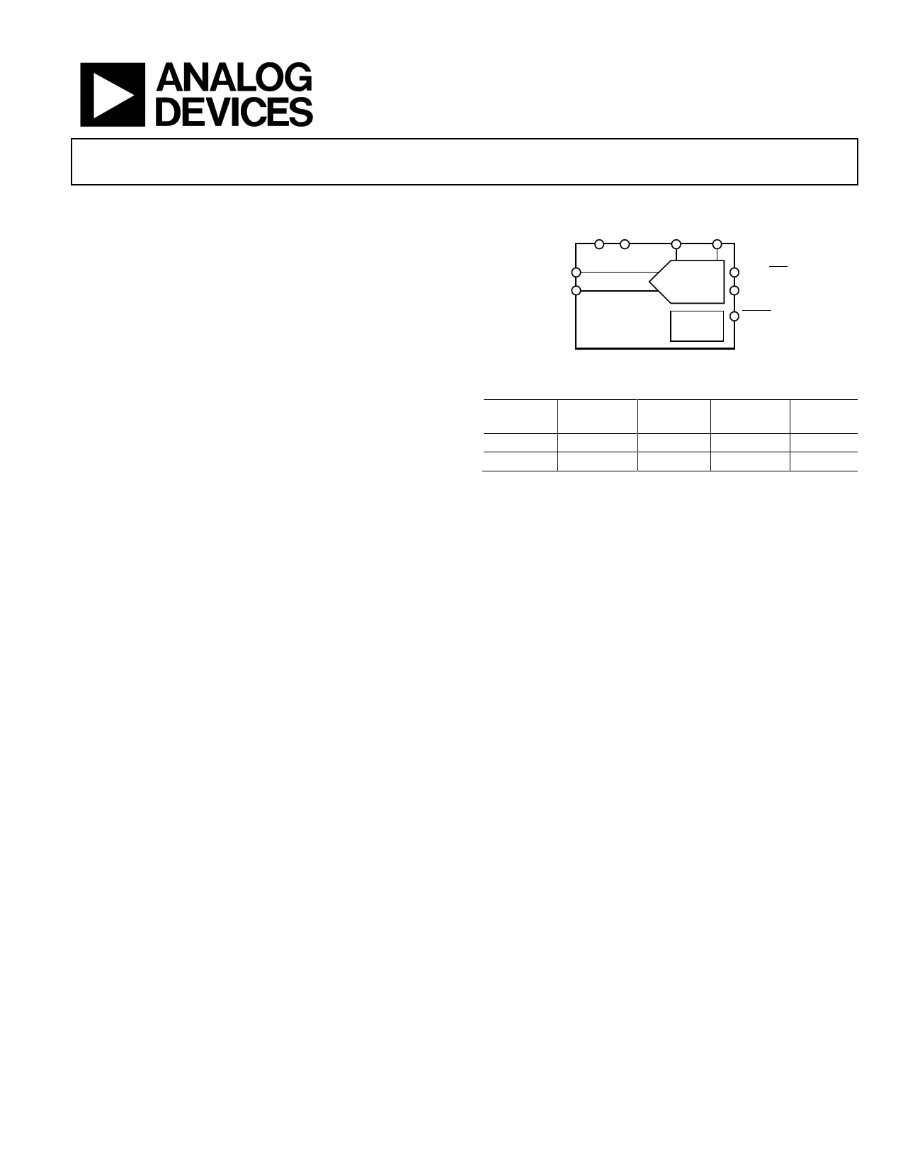
FUNCTIONAL BLOCK DIAGRAM
GND VDD
REFIN(+) REFIN(–)
AIN(+)
AIN(–)
12-BIT Σ-Δ
ADC
DOUT/RDY
SCLK
AD7170
INTERNAL
CLOCK
PDRST
Table 1.
VREF = VDD
5V
3V
Figure 1.
RMS Noise
11.5 μV
6.9 μV
P-P Noise
76 μV
45 μV
P-P
Resolution
12 bits
12 bits
ENOB
12 bits
12 bits
GENERAL DESCRIPTION
The AD7170 is a very low power 12-bit analog-to-digital converter
(ADC). It contains a precision 12-bit sigma-delta (Σ-Δ) ADC
and an on-chip oscillator. Consuming only 135 μA, the AD7170
is particularly suitable for portable or battery operated products
where very low power is a requirement. The AD7170 also has a
power-down mode in which the device consumes 5 μA, thus
increasing the battery life of the product.
For ease-of-use, all the features of the AD7170 are controlled by
dedicated pins. Each time a data read occurs, eight status bits
are appended to the 12-bit conversion. These status bits contain
a pattern sequence that can be used to confirm the validity of
the serial transfer.
The output data rate of the AD7170 is 125 Hz, whereas the
settling time is 24 ms. The AD7170 has one differential input
and a gain of 1. This is useful in applications where the user
needs to use an external amplifier to implement system-specific
filtering or gain requirements.
The AD7170 operates with a power supply from 2.7 V to 5.25 V.
It is available in a 10-lead LFCSP package.
The AD7171 is a 16-bit version of the AD7170. It has the same
feature set as the AD7170 and is pin-for-pin compatible.
Rev. B
Document Feedback
Information furnished by Analog Devices is believed to be accurate and reliable. However, no
responsibilityisassumedbyAnalogDevices for itsuse,nor foranyinfringementsofpatentsor other
rights of third parties that may result from its use. Specifications subject to change without notice. No
license is granted by implication or otherwise under any patent or patent rights of Analog Devices.
Trademarksandregisteredtrademarksarethepropertyoftheirrespectiveowners.
One Technology Way, P.O. Box 9106, Norwood, MA 02062-9106, U.S.A.
Tel: 781.329.4700 ©2009–2015 Analog Devices, Inc. All rights reserved.
Technical Support
www.analog.com
1 page 
AD7170
Parameter
LOGIC OUTPUT (DOUT/RDY)
Output High Voltage, VOH2
Output Low Voltage, VOL2
Min
VDD − 0.6
4
AD7170B1
Typ
Floating-State Leakage Current
Floating-State Output
Capacitance
Data Output Coding
POWER REQUIREMENTS3
Power Supply Voltage
VDD – GND
Power Supply Currents
IDD Current
IDD (Power-Down/Reset Mode)
Offset binary
2.7
±2
5
110
135
5
Max
0.4
0.4
5.25
130
150
Unit
V
V
V
V
µA
pF
V
µA
µA
µA
1 Temperature range is −40°C to +105°C.
2 Specification is not production tested but is supported by characterization data at initial product release.
3 Digital inputs equal to VDD or GND.
Data Sheet
Test Conditions/Comments
VDD = 3 V, ISOURCE = 100 µA
VDD = 5 V, ISOURCE = 200 µA
VDD = 3 V, ISINK = 100 µA
VDD = 5 V, ISINK = 1.6 mA
VDD = 3 V
VDD = 5 V
Rev. B | Page 4 of 14
5 Page 
AD7170
ADC CIRCUIT INFORMATION
OVERVIEW
The AD7170 is a low power ADC that incorporates a precision
12-bit Σ-∆ modulator and an on-chip digital filter intended for
measuring wide dynamic range, low frequency signals. The
device has an internal clock and one differential input. It
operates with an output data rate of 125 Hz and has a gain of 1.
A 2-wire interface simplifies data retrieval from the AD7170.
FILTER, DATA RATE, AND SETTLING TIME
The AD7170 uses a sinc3 filter. The output data rate is set to
125 Hz; thus, valid conversions are available every 1/125 = 8 ms.
If a reset occurs, then the user must allow the complete settling
time for the first conversion after the reset. The settling time is
equal to 24 ms. Subsequent conversions are available at 125 Hz.
When a step change occurs on the analog input, the AD7170
requires several conversion cycles to generate a valid conversion.
If the step change occurs synchronous to the conversion period,
then the settling time of the AD7170 must be allowed to generate
a valid conversion. If the step change occurs asynchronous to
the end of a conversion, then an extra conversion must be allowed
to generate a valid conversion. The data register is updated with
all the conversions but, for an accurate result, the user must
allow the required time.
Figure 12 shows the filter response of the filter. The only external
filtering required on the analog inputs is a simple R-C filter to
provide rejection at multiples of the master clock. A 1 KΩ
resistor in series with each analog input, a 0.01 μF capacitor
from each input to GND, and a 0.1 μF capacitor from AIN(+) to
AIN(−) are recommended.
0
–10
–20
–30
–40
–50
–60
–70
–80
–90
–100
0
125 250 375
500 625
INPUT SIGNAL FREQUENCY (Hz)
750
Figure 12. Filter Response
GAIN
The AD7170 has a gain of 1. The acceptable analog input range
is +VREF. Therefore, with VREF = 5 V, the input range is +5 V.
Data Sheet
POWER-DOWN/RESET (PDRST)
The PDRST pin functions as a power-down pin and a reset pin.
When PDRST is taken low, the AD7170 is powered down. The
entire ADC is powered down (including the on-chip clock), and
the DOUT/RDY pin is tristated. The circuitry and serial interface
are also reset. This resets the logic, the digital filter, and the analog
modulator. PDRST must be held low for 100 ns minimum to
initiate the reset function (see Figure 4).
When PDRST is taken high, the AD7170 is taken out of power-
down mode. When the on-chip clock has powered up (1 ms,
typically), the modulator then begins sampling the analog input.
The DOUT/RDY pin becomes active, going high until a valid
conversion is available. A reset is automatically performed on
power-up.
ANALOG INPUT CHANNEL
The AD7170 has one differential analog input channel that is
connected to the modulator; that is, the input is unbuffered.
Note that this unbuffered input path provides a dynamic load
to the driving source. Therefore, resistor/capacitor combinations
on the input pins can cause dc gain errors, depending on the
output impedance of the source that is driving the ADC input.
Table 7 shows the allowable external resistance/capacitance
values such that no gain error at the 12-bit level is introduced.
Table 7. External R-C Combination for No Gain Error
C (pF)
R (Ω)
50 9 k
100 6 k
500 1.5 k
1000
900
5000
200
The absolute input voltage range is restricted to a range between
GND − 30 mV and VDD + 30 mV. Care must be taken in setting up
the common-mode voltage to avoid exceeding these limits. Other-
wise, there is degradation in linearity and noise performance.
BIPOLAR CONFIGURATION
The AD7170 accepts a bipolar input range. A bipolar input
range does not imply that the part can tolerate negative voltages
with respect to system GND. Signals on the AIN(+) input are
referenced to the voltage on the AIN(−) input. For example, if
AIN(−) is 2.5 V, the analog input range on the AIN(+) input is
0 V to 5 V when a 2.5 V reference is used.
Rev. B | Page 10 of 14
11 Page | ||
| Páginas | Total 15 Páginas | |
| PDF Descargar | [ Datasheet AD7170.PDF ] | |
Hoja de datos destacado
| Número de pieza | Descripción | Fabricantes |
| AD7170 | 12-Bit Low Power Sigma-Delta ADC | Analog Devices |
| AD7171 | Sigma-Delta ADC | Analog Devices |
| AD7172-2 | Sigma-Delta ADC | Analog Devices |
| AD7173-8 | Highly Integrated Sigma-Delta ADC | Analog Devices |
| Número de pieza | Descripción | Fabricantes |
| SLA6805M | High Voltage 3 phase Motor Driver IC. |
Sanken |
| SDC1742 | 12- and 14-Bit Hybrid Synchro / Resolver-to-Digital Converters. |
Analog Devices |
|
DataSheet.es es una pagina web que funciona como un repositorio de manuales o hoja de datos de muchos de los productos más populares, |
| DataSheet.es | 2020 | Privacy Policy | Contacto | Buscar |