|
|
|
PDF AD5791-EP Data sheet ( Hoja de datos )
| Número de pieza | AD5791-EP | |
| Descripción | Voltage Output DAC | |
| Fabricantes | Analog Devices | |
| Logotipo | ||
Hay una vista previa y un enlace de descarga de AD5791-EP (archivo pdf) en la parte inferior de esta página. Total 20 Páginas | ||
|
No Preview Available !
Enhanced Product
1 ppm, 20-Bit,
±1 LSB INL, Voltage Output DAC
AD5791-EP
FEATURES
1 ppm resolution
1 ppm INL
7.5 nV/√Hz noise spectral density
0.19 LSB long-term linearity stability
<0.05 ppm/°C temperature drift
1 µs settling time
1.4 nV-sec glitch impulse
20-lead TSSOP package
Wide power supply range up to ±16.5 V
35 MHz Schmitt triggered digital interface
1.8 V compatible digital interface
Extended automotive operating temperature range: −55°C
to +125°C
ENHANCED PRODUCT FEATURES
Supports defense and aerospace applications (AQEC
standard)
Military temperature range (−55°C to +125°C)
Controlled manufacturing baseline
One assembly/test site
One fabrication site
Enhanced product change notification
Qualification data available on request
APPLICATIONS
Medical instrumentation
Test and measurement
Industrial control
High end scientific and aerospace instrumentation
GENERAL DESCRIPTION
The AD5791-EP1 is a single 20-bit, unbuffered voltage-output
DAC that operates from a bipolar supply of up to 33 V. The
AD5791 accepts a positive reference input in the range 5 V to
VDD − 2.5 V and a negative reference input in the range VSS +
2.5 V to 0 V. The AD5791-EP offers a relative accuracy
specification of ±1 LSB max, and operation is guaranteed
monotonic with a ±1 LSB DNL maximum specification.
The part uses a versatile 3-wire serial interface that operates at
clock rates up to 35 MHz and that is compatible with standard
SPI, QSPI™, MICROWIRE™, and DSP interface standards. The
part incorporates a power-on reset circuit that ensures the DAC
output powers up to 0 V in a known output impedance state
and remains in this state until a valid write to the device takes
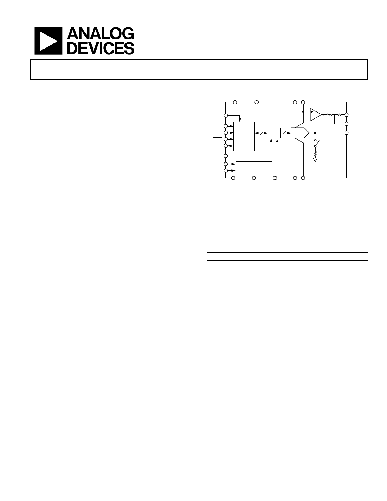
FUNCTIONAL BLOCK DIAGRAM
VCC
VDD
VREFPF VREFPS
IOVCC
SDIN
SCLK
SYNC
SDO
LDAC
CLR
RESET
AD5791-EP
INPUT
SHIFT
REGISTER
AND
CONTROL
LOGIC
20
DAC 20
REG
20-BIT
DAC
6.8kΩ 6.8kΩ
A1 RFB
R1 RFB
INV
VOUT
6kΩ
POWER-ON RESET
AND CLEAR LOGIC
DGND VSS AGND VREFNF VREFNS
Figure 1.
COMPANION PRODUCTS
Ultra precision op amps: AD8675, AD8676
High voltage op amp: ADA4898-1
Additional companion products on the AD5791 product page
Table 1. Related Device
Part No.
Description
AD5781
18-bit, 0.5 LSB INL, voltage output DAC
place. The part provides an output clamp feature that places the
output in a defined load state.
The AD5791-EP is available in a compact, 20-lead TSSOP
package and operates at the extended automotive temperature
range of −55°C to +125°C. Additional application and technical
information can be found in the AD5791 data sheet.
PRODUCT HIGHLIGHTS
1. 1 ppm Accuracy.
2. Wide Power Supply Range up to ±16.5 V.
3. Operating Temperature Range: −55°C to +125°C.
4. Low 7.5 nV/√Hz Noise Spectral Density.
5. Low 0.05 ppm/°C Temperature Drift.
1 Protected by U.S. Patents No. 7,884,747 and 8,089,380. Other patents pending.
Rev. A
Document Feedback
Information furnished by Analog Devices is believed to be accurate and reliable. However, no
responsibilityisassumedbyAnalogDevices for itsuse,nor foranyinfringementsofpatentsor other
rights of third parties that may result from its use. Specifications subject to change without notice. No
license is granted by implication or otherwise under any patent or patent rights of Analog Devices.
Trademarksandregisteredtrademarksarethepropertyoftheirrespectiveowners.
One Technology Way, P.O. Box 9106, Norwood, MA 02062-9106, U.S.A.
Tel: 781.329.4700 ©2012–2013 Analog Devices, Inc. All rights reserved.
Technical Support
www.analog.com
1 page 
Enhanced Product
AD5791-EP
TIMING CHARACTERISTICS
VCC = 2.7 V to 5.5 V; all specifications TMIN to TMAX, unless otherwise noted.
Table 3.
Parameter
t1 2
t2
t3
t4
t5
t6
t7
t8
t9
t10
t11
t12
t13
t14
t15
t16
t17
t18
t19
t20
t21
t22
Limit1
IOVCC = 1.71 V to 3.3 V IOVCC = 3.3 V to 5.5 V
40 28
92 60
15 10
95
55
22
48 40
86
97
12 7
13 10
20 16
14 11
130 130
130 130
50 50
140 140
00
65 60
62 45
00
35 35
150 150
Unit
ns min
ns min
ns min
ns min
ns min
ns min
ns min
ns min
ns min
ns min
ns min
ns min
ns min
ns typ
ns typ
ns min
ns typ
ns min
ns max
ns max
ns min
ns typ
ns typ
Test Conditions/Comments
SCLK cycle time
SCLK cycle time (readback mode)
SCLK high time
SCLK low time
SYNC to SCLK falling edge setup time
SCLK falling edge to SYNC rising edge hold time
Minimum SYNC high time
SYNC rising edge to next SCLK falling edge ignore
Data setup time
Data hold time
LDAC falling edge to SYNC falling edge
SYNC rising edge to LDAC falling edge
LDAC pulse width low
LDAC falling edge to output response time
SYNC rising edge to output response time (LDAC tied low)
CLR pulse width low
CLR pulse activation time
SYNC falling edge to first SCLK rising edge
SYNC rising edge to SDO tristate (CL = 50 pF)
SCLK rising edge to SDO valid (CL = 50 pF)
SYNC rising edge to SCLK rising edge ignore
RESET pulse width low
RESET pulse activation time
1 All input signals are specified with tR = tF = 1 ns/V (10% to 90% of IOVCC) and timed from a voltage level of (VIL + VIH)/2.
2 Maximum SCLK frequency is 35 MHz for write mode and 16 MHz for readback mode.
Rev. A | Page 5 of 20
5 Page 
Enhanced Product
0.4
DNL MAX
0.3
0.2
0.1
0
–0.1
TA = 25°C
VREFP = +10V
VREFN = –10V
AD8676 REFERENCE BUFFERS
AD8675 OUTPUT BUFFER
–0.2
–0.3
DNL MIN
–0.4
12.5 13.0 13.5 14.0 14.5 15.0 15.5 16.0 16.5
VDD/|VSS| (V)
Figure 17. Differential Nonlinearity Error vs. Supply Voltage, ±10 V Span
0.4
DNL MAX
0.2
0
–0.2
–0.4
TA = 25°C
VREFP = +5V
VREFN = 0V
AD8676 REFERENCE BUFFERS
AD8675 OUTPUT BUFFER
–0.6
–0.8
DNL MIN
–1.0
7.5 8.5 9.5 10.5 11.5 12.5 13.5 14.5 15.5 16.5
VDD (V)
–2.5 –3.9 –5.3 –6.7 –9.1 –10.5 –12.9 –14.2 –15.5 –16.5
VSS (V)
Figure 18. Differential Nonlinearity Error vs. Supply Voltage, 5 V Span
0.6
0.5
0.4
0.3
TA = 25°C
0.2
VREFP = +10V
VREFN = –10V
AD8676 REFERENCE BUFFERS
AD8675 OUTPUT BUFFER
0.1
0
12.5 13.0 13.5 14.0 14.5 15.0 15.5 16.0 16.5
VDD/|VSS| (V)
Figure 19. Zero-Scale Error vs. Supply Voltage, ±10 V Span
AD5791-EP
0.6
TA = 25°C
VREFP = +5V
0.5 VREFN = 0V
AD8676 REFERENCE BUFFERS
AD8675 OUTPUT BUFFER
0.4
0.3
0.2
0.1
0
7.5 8.5 9.5 10.5 11.5 12.5 13.5 14.5 15.5 16.5
VDD (V)
–2.5 –3.9 –5.3 –6.7 –9.1 –10.5 –12.9 –14.2 –15.5 –16.5
VSS (V)
Figure 20. Zero-Scale Error vs. Supply Voltage, 5 V Span
0.20
0.15
TA = 25°C
VREFP = +10V
VREFN = –10V
AD8676 REFERENCE BUFFERS
AD8675 OUTPUT BUFFER
0.10
0.05
0
–0.05
–0.10
–0.15
12.5 13.0 13.5 14.0 14.5 15.0 15.5 16.0
VDD/|VSS| (V)
Figure 21. Midscale Error vs. Supply Voltage, ±10 V Span
16.5
0.2
0.1
0
–0.1
–0.2
–0.3
–0.4
TA = 25°C
–0.5
VREFP = +5V
VREFN = 0V
–0.6
AD8676 REFERENCE BUFFERS
AD8675 OUTPUT BUFFER
–0.7
7.5 8.5 9.5 10.5 11.5 12.5 13.5 14.5 15.5 16.5
VDD (V)
–2.5 –3.9 –5.3 –6.7 –9.1 –10.5 –12.9 –14.2 –15.5 –16.5
VSS (V)
Figure 22. Midscale Error vs. Supply Voltage, 5 V Span
Rev. A | Page 11 of 20
11 Page | ||
| Páginas | Total 20 Páginas | |
| PDF Descargar | [ Datasheet AD5791-EP.PDF ] | |
Hoja de datos destacado
| Número de pieza | Descripción | Fabricantes |
| AD5791-EP | Voltage Output DAC | Analog Devices |
| Número de pieza | Descripción | Fabricantes |
| SLA6805M | High Voltage 3 phase Motor Driver IC. |
Sanken |
| SDC1742 | 12- and 14-Bit Hybrid Synchro / Resolver-to-Digital Converters. |
Analog Devices |
|
DataSheet.es es una pagina web que funciona como un repositorio de manuales o hoja de datos de muchos de los productos más populares, |
| DataSheet.es | 2020 | Privacy Policy | Contacto | Buscar |