|
|
|
PDF AD5721 Data sheet ( Hoja de datos )
| Número de pieza | AD5721 | |
| Descripción | Voltage Output DAC | |
| Fabricantes | Analog Devices | |
| Logotipo | ||
Hay una vista previa y un enlace de descarga de AD5721 (archivo pdf) en la parte inferior de esta página. Total 30 Páginas | ||
|
No Preview Available !
Data Sheet
Multiple Range, 16-/12-Bit,
Bipolar/Unipolar, Voltage Output DACs
AD5761/AD5721
FEATURES
8 software-programmable output ranges: 0 V to 5 V, 0 V to 10 V,
0 V to 16 V, 0 V to 20 V, ±3 V, ±5 V, ±10 V, −2.5 V to +7.5 V;
5% overrange
Total unadjusted error (TUE): 0.1% FSR maximum
16-bit resolution: ±2 LSB maximum INL
Guaranteed monotonicity: ±1 LSB maximum
Single channel, 16-/12-bit DACs
Settling time: 7.5 µs typical
Integrated reference buffers
Low noise: 35 nV/√Hz
Low glitch: 1 nV-sec
1.8 V logic compatibility
Asynchronous updating via LDAC
Asynchronous RESET to zero scale/midscale
DSP/microcontroller-compatible serial interface
Robust 4 kV HBM ESD rating
Available in 16-lead TSSOP and 16-lead LFCSP
Operating temperature range: −40°C to +125°C
APPLICATIONS
Industrial automation
Instrumentation, data acquisition
Open-/closed-loop servo control, process control
Programmable logic controllers
GENERAL DESCRIPTION
The AD5761/AD5721 are single channel, 16-/12-bit serial input,
voltage output, digital-to-analog converters (DACs). They operate
from single supply voltages from 4.75 V to 30 V or dual supply
voltages from −16.5 V to 0 V VSS and 4.75 V to 16.5 V VDD. The
integrated output amplifier and reference buffer provide a very
easy to use, universal solution.
The devices offer guaranteed monotonicity, integral nonlinearity
(INL) of ±2 LSB maximum, 35 nV/√Hz noise, and 7.5 µs settling
time on selected ranges.
The AD5761/AD5721 use a serial interface that operates at
clock rates of up to 50 MHz and are compatible with DSP and
microcontroller interface standards. Double buffering allows
the asynchronous updating of the DAC output. The input
coding is user-selectable twos complement or straight binary.
The asynchronous reset function resets all registers to their
default state. The output range is user selectable, via the
RA[2:0] bits in the control register.
The devices available in the 16-lead TSSOP and in the 16-lead
LFCSP offer guaranteed specifications over the −40°C to +125°C
industrial temperature range.
Table 1. Pin-Compatible Devices
Device
Description
AD5761R/AD5721R AD5761/AD5721 with internal reference
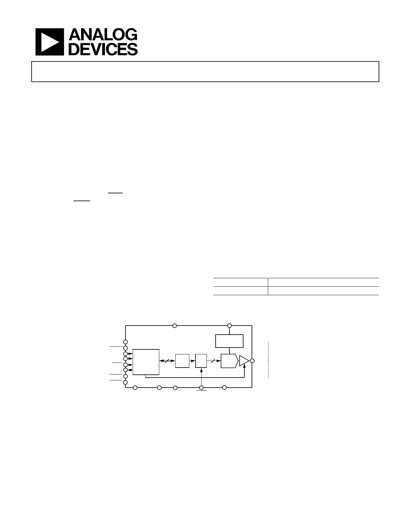
FUNCTIONAL BLOCK DIAGRAM
VDD
VREFIN
DVCC
ALERT
SDI
SCLK
SYNC
SDO
RESET
CLEAR
AD5761/AD5721
INPUT SHIFT
REGISTER
AND
CONTROL
LOGIC
12/16
INPUT
REG
REFERENCE
BUFFERS
DAC 12/16 12-BIT/
REG
16-BIT
DAC
DNC
DGND VSS
LDAC
AGND
NOTES
1. DNC = DO NOT CONNECT. DO NOT CONNECT TO THIS PIN.
Figure 1.
VOUT
0V TO 5V
0V TO 10V
0V TO 16V
0V TO 20V
±3V
±5V
±10V
−2.5V TO +7.5V
Rev. B
Document Feedback
Information furnished by Analog Devices is believed to be accurate and reliable. However, no
responsibility is assumed by Analog Devices for its use, nor for any infringements of patents or other
rights of third parties that may result from its use. Specifications subject to change without notice. No
license is granted by implication or otherwise under any patent or patent rights of Analog Devices.
Trademarksandregisteredtrademarksarethepropertyoftheirrespectiveowners.
One Technology Way, P.O. Box 9106, Norwood, MA 02062-9106, U.S.A.
Tel: 781.329.4700 ©2015–2016 Analog Devices, Inc. All rights reserved.
Technical Support
www.analog.com
1 page 
Data Sheet
AD5761/AD5721
AC PERFORMANCE CHARACTERISTICS
VDD1 = 4.75 V to 30 V, VSS1= −16.5 V to 0 V, AGND = DGND = 0 V, VREFIN = 2.5 V external, DVCC = 1.7 V to 5.5 V, RLOAD = 1 kΩ for all
ranges except 0 V to 16 V and 0 V to 20 V for which RLOAD = 2 kΩ, CLOAD = 200 pF, all specifications TMIN to TMAX, unless otherwise noted.
Table 3.
Parameter2
DYNAMIC PERFORMANCE3
Output Voltage Settling Time
Digital-to-Analog Glitch Impulse
Glitch Impulse Peak Amplitude
Power-On Glitch
Digital Feedthrough
Output Noise
0.1 Hz to 10 Hz Bandwidth (BW)
100 kHz BW
Output Noise Spectral Density (at 10 kHz)
Total Harmonic Distortion (THD)4
Signal-to-Noise Ratio (SNR)
Peak Harmonic or Spurious Noise (SFDR)
Signal-to-Noise-and-Distortion
(SINAD) Ratio
Min Typ Max Unit
Test Conditions/Comments
9 12.5 µs
20 V step to 1 LSB at 16-bit resolution
7.5 8.5 µs
10 V step to 1 LSB at 16-bit resolution
5 µs
512 LSB step to 1 LSB at 16-bit resolution
8 nV-sec ±10 V range
1 nV-sec 0 V to 5 V range
15 mV ±10 V range
10 mV 0 V to 5 V range
100 mV p-p
0.6 nV-sec
15 µV p-p
45 µV rms 0 V to 20 V and 0 V to 16 V ranges, 2.5 V external reference
35 µV rms 0 V to 10 V, ±10 V, −2.5 V to +7.5 V ranges, 2.5 V external
reference
25 µV rms ±5 V range, 2.5 V external reference
15 µV rms +5 V, ±3 V ranges; 2.5 V external reference
80 nV/√Hz ±10 V range, 2.5 V external reference
35 nV/√Hz ±3 V range, 2.5 V external reference
70 nV/√Hz ±5 V, 0 V to 10 V, and −2.5 V to +7.5 V ranges; 2.5 V external
reference
110 nV/√Hz 0 V to 20 V range, 2.5 V external reference
90 nV/√Hz 0 V to 16 V range, 2.5 V external reference
45 nV/√Hz 0 V to 5 V range, 2.5 V external reference
−87 dB 2.5 V external reference, 1 kHz tone
92 dB At ambient, 2.5 V external reference, BW = 20 kHz, fOUT = 1 kHz
92 dB At ambient, 2.5 V external reference, BW = 20 kHz, fOUT = 1 kHz
85 dB At ambient, 2.5 V external reference, BW = 20 kHz, fOUT = 1 kHz
1 For specified performance, headroom requirement is 1 V.
2 Temperature range: −40°C to +125°C, typical at +25°C.
3 Guaranteed by design and characterization; not production tested.
4 Digitally generated sine wave at 1 kHz.
Rev. B | Page 5 of 31
5 Page 
Data Sheet
1.0
±3V SPAN
0.8
±5V SPAN
±10V SPAN
–2.5V TO +7.5V SPAN
0.6
0.4
0.2
0
–0.2
–0.4
–0.6
–0.8 VDD = +21V
–1.0 VSS = –11V
0 10000
20000 30000 40000
DAC CODE
50000
60000
Figure 13. AD5761 DNL Error vs. DAC Code, Bipolar Output
0.5
0.4
0.3
0.2
0.1
0
–0.1
–0.2
–0.3
–0.4
–0.5
0
±3V SPAN
±5V SPAN
±10V SPAN
–2.5V TO +7.5V SPAN
VDD = +21V
VSS = –11V
500 1000 1500 2000 2500 3000 3500 4000
DAC CODE
Figure 14. AD5721 DNL Error vs. DAC Code, Bipolar Output
2.0
MAXIMUM INL, 0V TO 5V SPAN
MAXIMUM INL, ±10V SPAN
1.5 MINIMUM INL, 0V TO 5V SPAN
MINIMUM INL, ±10V SPAN
1.0
VDD = +21V
VSS = –11V
0.5
0
–0.5
–1.0
–1.5
–2.0
–40
–20
0 25 50 85
TEMPERATURE (°C)
105 125
Figure 15. INL Error vs. Temperature
AD5761/AD5721
1.0
MAXIMUM DNL, 0V TO 5V SPAN
0.8
MAXIMUM DNL, ±10V SPAN
MINIMUM DNL, 0V TO 5V SPAN
MINIMUM DNL, ±10V SPAN
0.6
VDD = +21V
VSS = –11V
0.4
0.2
0
–0.2
–0.4
–0.6
–0.8
–1.0
–40
–20 0
25 50 85 105
TEMPERATURE (°C)
Figure 16. DNL Error vs. Temperature
125
2.0
MAXIMUM INL, 0V TO 5V SPAN
MAXIMUM INL, ±10V SPAN
1.5 MINIMUM INL, 0V TO 5V SPAN
MINIMUM INL, ±10V SPAN
1.0
VDD = +21V
TVASS==25–°1C1V
NO LOAD
0.5
0
–0.5
–1.0
–1.5
–2.0
+5V SPAN AVDD/AVSS = +6V/–1V
±10V SPAN AVDD/AVSS = +11V/–11V
AVDD/AVSS = +10V/–1V
AVDD/AVSS = +13.5V/–13.5V
AVDD/AVSS = +16.5V/–1V
AVDD/AVSS = +16.5V/–16.5V
AVDD/AVSS = +7.5V/–1V
AVDD/AVSS = +12.5V/–12.5V
AVDD/AVSS = +12.5V/–1V
AVDD/AVSS = +14.5V/–14.5V
SUPPLY VOLTAGE (V)
Figure 17. INL Error vs. Supply Voltage
1.0
MAXIMUM DNL, 0V TO 5V SPAN
0.8
MAXIMUM DNL, ±10V SPAN
MINIMUM DNL, 0V TO 5V SPAN
MINIMUM DNL, ±10V SPAN
0.6
VDD = +21V
VTASS==25–°1C1V
NO LOAD
0.4
0.2
0
–0.2
–0.4
–0.6
–0.8
–1.0
+5V SPAN AVDD/AVSS = +6V/–1V
±10V SPAN AVDD/AVSS = +11V/–11V
AVDD/AVSS = +10V/–1V
AVDD/AVSS = +13.5V/–13.5V
AVDD/AVSS = +16.5V/–1V
AVDD/AVSS = +16.5V/–16.5V
AVDD/AVSS = +7.5V/–1V
AVDD/AVSS = +12.5V/–12.5V
AVDD/AVSS = +12.5V/–1V
AVDD/AVSS = +14.5V/–14.5V
SUPPLY VOLTAGE (V)
Figure 18. DNL Error vs. Supply Voltage
Rev. B | Page 11 of 31
11 Page | ||
| Páginas | Total 30 Páginas | |
| PDF Descargar | [ Datasheet AD5721.PDF ] | |
Hoja de datos destacado
| Número de pieza | Descripción | Fabricantes |
| AD572 | 12-BIT SUCCESSIVE APPROXIMATION INTEGRATED CIRCUIT A/D CONVERTER | Analog Devices |
| AD5721 | Voltage Output DAC | Analog Devices |
| AD5721R | Bipolar/Unipolar Voltage Output DACs | Analog Devices |
| AD5722 | (AD57x2) Voltage Output DACs | Analog Devices |
| Número de pieza | Descripción | Fabricantes |
| SLA6805M | High Voltage 3 phase Motor Driver IC. |
Sanken |
| SDC1742 | 12- and 14-Bit Hybrid Synchro / Resolver-to-Digital Converters. |
Analog Devices |
|
DataSheet.es es una pagina web que funciona como un repositorio de manuales o hoja de datos de muchos de los productos más populares, |
| DataSheet.es | 2020 | Privacy Policy | Contacto | Buscar |