|
|
|
PDF ADP1850 Data sheet ( Hoja de datos )
| Número de pieza | ADP1850 | |
| Descripción | DC-to-DC Synchronous Buck Controller | |
| Fabricantes | Analog Devices | |
| Logotipo | ||
Hay una vista previa y un enlace de descarga de ADP1850 (archivo pdf) en la parte inferior de esta página. Total 30 Páginas | ||
|
No Preview Available !
Data Sheet
Wide Range Input, Dual/Two-Phase, DC-to-DC
Synchronous Buck Controller
ADP1850
FEATURES
Wide range input: 2.75 V to 20 V
Power stage input voltage: 1 V to 20 V
Output voltage range: 0.6 V up to 90% VIN
Output current to more than 25 A per channel
Accurate current sharing between channels (interleaved)
Programmable frequency: 200 kHz to 1.5 MHz
180° phase shift between channels for reduced input
capacitance
±0.85% reference voltage accuracy from −40°C to +85°C
Integrated boost diodes
Power saving mode (PSM) at light loads
Accurate power good with internal pull-up resistor
Accurate voltage tracking capability
Independent channel precision enable
Overvoltage and overcurrent limit protection
Externally programmable soft start, slope compensation and
current sense gain
Synchronization input
Thermal overload protection
Input undervoltage lockout (UVLO)
Available in 32-lead 5 mm × 5 mm LFCSP
APPLICATIONS
High current single and dual output intermediate bus and
point of load converters requiring sequencing and
tracking capability, including converters for:
Point-of-load power supplies
Telecom base station and networking
Consumer
Industrial and instrumentation
Healthcare and medical
GENERAL DESCRIPTION
The ADP1850 is a configurable dual output or two-phase, single
output dc-to-dc synchronous buck controller capable of running
from commonly used 3.3 V to 12 V (up to 20 V) voltage inputs.
The device operates in current mode for improved transient
response and uses valley current sensing for enhanced noise
immunity.
The architecture enables accurate current sharing between
interleaved phases for high current outputs.
The ADP1850 is ideal in system applications requiring multiple
output voltages: the ADP1850 includes a synchronization fea-
ture to eliminate beat frequencies between switching devices;
provides accurate tracking capability between supplies and
includes precision enable for simple, robust sequencing.
Rev. B
Document Feedback
Information furnished by Analog Devices is believed to be accurate and reliable. However, no
responsibility is assumed by Analog Devices for its use, nor for any infringements of patents or other
rights of third parties that may result from its use. Specifications subject to change without notice. No
license is granted by implication or otherwise under any patent or patent rights of Analog Devices.
Trademarksandregisteredtrademarksarethepropertyoftheirrespectiveowners.
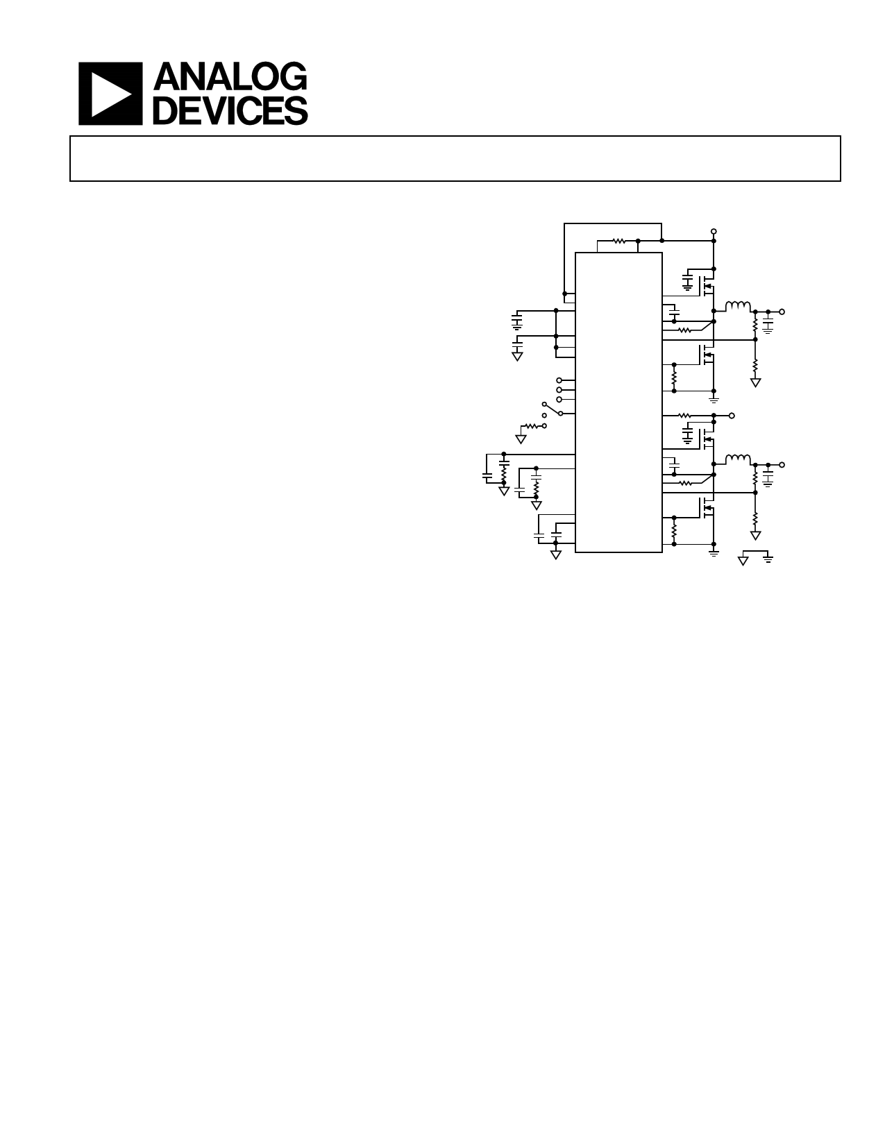
TYPICAL OPERATION CIRCUIT
RRAMP1
VIN
RAMP1 VIN
ADP1850
EN1
EN2
VDL
DH1
BST1
M1
L1
VCCO
TRK1
TRK2
SW1
ILIM1
FB1
DL1
R11
M2
R12
PGOOD1
RCSG1
PGOOD2 PGND1
HI
LO
SYNC
FREQ
RRAMP2
RAMP2
VIN
COMP1
COMP2
SS1
SS2
AGND
DH2
BST2
SW2
ILIM2
FB2
DL2
PGND2
M3
L2
R21
RCSG2
M4
R22
VOUT1
VOUT2
Figure 1. Single Phase Circuit
The ADP1850 provides high speed, high peak current drive
capability with dead-time optimization to enable energy
efficient power conversion. For low load operation, the device
can be configured to operate in power saving mode (PSM) by
skipping pulses and reducing switching losses to improve the
energy efficiency at light load and standby conditions.
The accurate current limit (±6%) allows the power architect to
design within a narrower range of tolerances and can reduce
overall converter size and cost.
The ADP1850 provides a configurable architecture capable
of wide range input operation to provide the designer with
maximum re-use opportunities and improved time to market.
Additional flexibility is provided by external programmability
of loop compensation, soft start, frequency setting, power
saving mode, current limit and current sense gain can all be
programmed using external components.
The ADP1850 includes a high level of integration in a small size
package. The start-up linear regulator and the boot-strap diode
for the high side drive are included. Protection features include:
undervoltage lock-out, overvoltage, overcurrent/short-circuit
and over temperature. The ADP1850 is available in a compact
32-lead LFCSP 5 mm × 5 mm thermally enhanced package.
One Technology Way, P.O. Box 9106, Norwood, MA 02062-9106, U.S.A.
Tel: 781.329.4700 ©2010–2017 Analog Devices, Inc. All rights reserved.
Technical Support
www.analog.com
1 page 
ADP1850
Data Sheet
Parameter
GATE DRIVERS
DHx Rise Time
DHx Fall Time
DLx Rise Time
DLx Fall Time
DHx to DLx Dead Time
DHx or DLx Driver RON, Sourcing
Current1
Symbol
RON_SOURCE
DHx or DLx Driver RON, Tempco
DHx or DLx Driver RON, Sinking
Current1
TCRON
RON_SINK
DHx Maximum Duty Cycle
DHx Maximum Duty Cycle
Minimum DHx On Time
Minimum DHx Off Time
Minimum DLx On Time
COMPx VOLTAGE RANGE
COMPx Pulse Skip Threshold
COMPx Clamp High Voltage
THERMAL SHUTDOWN
Thermal Shutdown Threshold
Thermal Shutdown Hysteresis
OVERVOLTAGE AND POWER GOOD
THRESHOLDS
FBx Overvoltage Threshold
FBx Overvoltage Hysteresis
FBx Undervoltage Threshold
FBx Undervoltage Hysteresis
TRKx INPUT VOLTAGE RANGE
FBx TO TRKx OFFSET VOLTAGE
SOFT START
SSx Output Current
SSx Pull-Down Resistor
FBx to SSx Offset
PGOODx
PGOODx Pull-up Resistor
PGOODx Delay
Over Voltage or Under Voltage
VCOMP,THRES
VCOMP,HIGH
TTMSD
VOV
VUV
ISS
RPGOOD
Minimum Duration
ILIM1, ILIM2 Threshold Voltage1
ILIM1, ILIM2 Output Current
Current Sense Blanking Period
INTEGRATED RECTIFIER
(BOOST DIODE) RESISTANCE
ZERO CURRENT CROSS OFFSET
(SWx TO PGNDx)1
1 Guaranteed by design.
2 Connect VIN to VCCO when 2.75 V < VIN < 5.5 V.
Conditions
CDH = 3 nF, VBST − VSW = 5 V
CDH = 3 nF, VBST − VSW = 5 V
CDL = 3 nF
CDL = 3 nF
External 3 nF is connected to DHx and DLx
Sourcing 2 A with a 100 ns pulse
Sourcing 1 A with a 100 ns pulse, VIN = 3 V
VIN = 3 V or 12 V
Sinking 2 A with a 100 ns pulse
Sinking 1 A with a 100 ns pulse, VIN = 3 V
fSW = 300 kHz
fSW = 1500 kHz
fSW = 200 kHz to 1500 kHz
fSW = 200 kHz to 1500 kHz
fSW = 200 kHz to 1500 kHz
In pulse skip mode
Min Typ
16
14
16
14
25
2
2.3
0.3
1.5
2
90
50
0.9
2.25
155
20
VFB rising
VFB falling
TRKx = 0.1 V to 0.57 V, offset = VFB − VTRK
0.635
0.525
0
−10
0.65
30
0.55
30
0
During start-up
During a fault condition
VSS = 0.1 V to 0.6 V, offset = VFB − VSS
4.6 6.5
3
−10
Internal pull-up resistor to VCCO
This is the minimum duration required to trip
the PGOOD signal
12.5
12
10
Relative to PGNDx
ILIMx = PGNDx
After DLx goes high, current limit is not sensed
during this period
At 20 mA forward current
−5
47
0
50
100
16
In pulse skip mode only, fSW = 600 kHz
02
Max Unit
ns
ns
ns
ns
ns
Ω
Ω
%/oC
Ω
Ω
%
%
135 ns
335 ns
285 ns
V
V
C
C
0.665
0.578
5
+10
V
mV
V
mV
V
mV
8.4 μA
kΩ
+10 mV
kΩ
μs
μs
+5 mV
53 μA
ns
Ω
4 mV
Rev. B | Page 4 of 32
5 Page 
ADP1850
OUTPUT RESPONSE
1
8A TO 13A STEP LOAD
4 VIN = 12V
VOUT = 3.3V
CH1 20mV BW
CH4 5A Ω
M200µs
A CH4 11.5A
Figure 10. Step Load Transient of Figure 44
1
2
VOUT1
DH1
DL1
3 IL1
4
VIN = 12V
VOUT = 1.8V
OUTPUT PRECHARGED TO 1V
CH1 5V
CH3 1V
CH2 5V
CH4 1A Ω
M1ms
A CH1 2.4V
Figure 11. Soft Start into Precharged Output
1
SW
VOUT (CH3)
EN
3
2
4
SS (CH4)
CH1 10V
CH3 1V
CH2 2V
CH4 1V
M10ms
CSS = 100nF
A CH2 1.52V
Figure 12. Enable Start-Up Function
Data Sheet
SW1
1
PGOOD1
VCCO (CH3)
2
3 VOUT, PRELOADED (CH4)
4
CH1 10V
CH3 2V
CH2 2V
CH4 2V Ω
M10ms
A CH2 3.76V
Figure 13. Thermal Shutdown Waveform
0.5
REFERENCED AT VIN = 2.75V
0
–0.5
600kHz
–1.0
300kHz
–1.5
–2.0
–2.5
3
850kHz
5 7 9 11 13 15 17 19 21
VIN (V)
Figure 14. Change in fSW vs. VIN
2.0
1.5
1.0
0.5
0
–0.5
–1.0
–1.5
–2.0
–2.5
–40
VIN = 12V; REFERENCED AT 25°C
–15 10 35 60 85
TEMPERATURE (°C)
Figure 15. fSW vs. Temperature
110 135
Rev. B | Page 10 of 32
11 Page | ||
| Páginas | Total 30 Páginas | |
| PDF Descargar | [ Datasheet ADP1850.PDF ] | |
Hoja de datos destacado
| Número de pieza | Descripción | Fabricantes |
| ADP1850 | DC-to-DC Synchronous Buck Controller | Analog Devices |
| ADP1850 | DC-to-DC Synchronous Buck Controller | Analog Integrations Corporation |
| ADP1851 | Step-Down DC-to-DC Controller | Analog Devices |
| ADP1853 | Step-Down DC-to-DC Controller | Analog Devices |
| Número de pieza | Descripción | Fabricantes |
| SLA6805M | High Voltage 3 phase Motor Driver IC. |
Sanken |
| SDC1742 | 12- and 14-Bit Hybrid Synchro / Resolver-to-Digital Converters. |
Analog Devices |
|
DataSheet.es es una pagina web que funciona como un repositorio de manuales o hoja de datos de muchos de los productos más populares, |
| DataSheet.es | 2020 | Privacy Policy | Contacto | Buscar |