|
|
|
PDF NJG1133MD7 Data sheet ( Hoja de datos )
| Número de pieza | NJG1133MD7 | |
| Descripción | UMTS Triple Band LNA GaAs MMIC | |
| Fabricantes | New Japan Radio | |
| Logotipo | ||
Hay una vista previa y un enlace de descarga de NJG1133MD7 (archivo pdf) en la parte inferior de esta página. Total 30 Páginas | ||
|
No Preview Available !
NJG1133MD7
UMTS Triple Band LNA GaAs MMIC
IGENERAL DISCRIPTION
NJG1133MD7 is a triple band LNA IC designed for UMTS and LTE.
This IC has a LNA pass-through function to select high gain mode
or suitable low gain mode. The LNA of 1.7GHz band can be used
to 1.5GHz band by changing application circuit.
An ultra-small and ultra-thin package of EQFN14-D7 is adopted.
IPACKAGE OUTLINE
NJG1133MD7
IAPPLICATIONS
2.1GHz, 1.7GHz and 800MHz triple band of standard condition application
Any dual High-band and single Low-band combination for LTE and UMTS applications,
like Band1,2 and 5,Band1,3 and 5,Band1,2 and 8
Note: For except of standard condition applications please refer to Application Note
IFEATURES
GLow operation voltage
GLow control voltage
GLow current consumption
GSmall and thin package
[High Gain Mode]
●High gain
●Low noise figure
●High input IP3
[Low Gain Mode]
●Gain
●High input IP3
+2.8V typ.
+1.8V typ.
2.3mA typ. @High Gain Mode
48µA typ. @Low Gain Mode
EQFN14-D7 (Package size: 1.6 x 1.6 x 0.397mm typ.)
16.0dB typ.
1.35dB typ.
1.40dB typ.
1.55dB typ.
+0.5dBm typ.
-2.0dBm typ.
0dBm typ.
0dBm typ.
@fRF=2140MHz, 885MHz, 1860MHz, 1495MHz
@fRF=2140MHz, 1860MHz
@fRF=885MHz
@fRF=1495MHz
@fRF=2140.0+2140.1MHz, Pin=-30dBm
@fRF=885.0+885.1MHz, Pin=-30dBm
@fRF=1860.0+1860.1MHz, Pin=-30dBm
@fRF=1495.0+1495.1MHz, Pin=-30dBm
-3.5dB typ.
-3.0dB typ.
-4.0dB typ.
+12dBm typ.
+12dBm typ.
+15dBm typ.
+15dBm typ.
@fRF=2140MHz
@fRF=885MHz, 1495MHz
@fRF=1860MHz
@fRF=2140.0+2140.1MHz, Pin=-16dBm
@fRF=885.0+885.1MHz, Pin=-20dBm
@fRF=1860.0+1860.1MHz, Pin=-16dBm
@fRF=1495.0+1495.1MHz, Pin=-16dBm
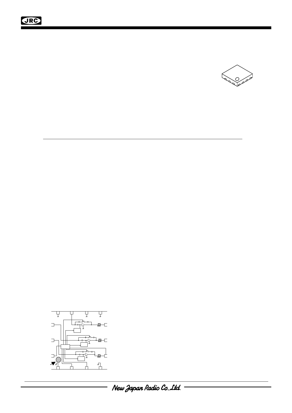
IPIN CONFIGURATION
GND 11
RFIN3 10
(Top View)
GND 9
GND 8
RFIN2
132
RFIN1
13
VCTL3
14
1pin
GND 1
Bias
Circuit
1.71G.H7zGBaHndz
Band
Logic
Circuit
2.1GHz Band
Bias
Circuit
800MHz Band
Bias
Circuit
RFOUT3
7
RFOUT2
6
5
RFOUT1
VCTL2 2
VCTL1 3
GND 4
Pin Connection
1. GND
2. VCTL2
3. VCTL1
4. GND
5. RFOUT1 (800MHz)
6. RFOUT2 (2.1GHz)
7. RFOUT3 (1.7G/1.5GHz)
8. GND
9. GND
10. RFIN3 (1.7G/1.5GHz)
11. GND
12. RFIN2 (2.1GHz)
13. RFIN1 (800MHz)
14. VCTL3
Note: Specifications and description listed in this datasheet are subject to change without prior notice.
Ver.2013-04-23
-1-
1 page 
NJG1133MD7
IELECTRICAL CHARACTERISTICS 6 (1.7GHz Band High Gain Mode)
General conditions: VDD=2.7V, VCTL1=0V, VCTL2=1.8V, VCTL3=1.8V, fRF=1860MHz, Ta=+25°C,
Zs=Zl=50Ω, with application circuit
PARAMETERS
SYMBOL
CONDITIONS
MIN TYP MAX UNITS
Small signal gain 5
Gain5
Exclude PCB & connector losses
(IN: 0.10dB, OUT: 0.31dB)
Noise figure 5
NF5
Exclude PCB & connector losses
(IN: 0.10dB)
Input Power at 1dB gain
compression point 5
P-1dB(IN)_5
Input 3rd order intercept
point 5
IIP3_5
f1=fRF, f2=fRF+100kHz,
Pin=-30dBm
14.5 16.0
- 1.35
-16.0 -8.0
-9.0 0
17.5 dB
1.6 dB
- dBm
- dBm
RF Input VSWR 5
VSWRi5
- 2.1 2.6
RF Output VSWR 5
VSWRo5
- 1.8 2.2
IELECTRICAL CHARACTERISTICS 7 (1.7GHz Band Low Gain Mode)
General conditions: VDD=2.7V, VCTL1=0V, VCTL2=1.8V, VCTL3=0V, fRF=1860MHz, Ta=+25°C,
Zs=Zl=50Ω, with application circuit
PARAMETERS
SYMBOL
CONDITIONS
MIN TYP MAX UNITS
Small signal gain 6
Gain6
Exclude PCB & connector losses
(IN: 0.10dB, OUT: 0.31dB)
Noise figure 6
NF6
Exclude PCB & connector losses
(IN: 0.10dB)
Input Power at 1dB gain
compression point 6
P-1dB(IN)_6
Input 3rd order intercept
point 6
IIP3_6
f1=fRF, f2=fRF+100kHz,
Pin=-16dBm
RF Input VSWR 6
VSWRi6
-5.5
-
+4.0
0
-
-4.0
4.0
+16.0
+15.0
1.7
-2.0 dB
6.5 dB
- dBm
- dBm
2.2
RF Output VSWR 6
VSWRo6
- 2.4 2.7
-5-
5 Page 
IELECTRICAL CHARACTERISTICS (2.1GHz band High Gain mode)
2.1GHz @High Gain
IDD vs. VDD
4
3.5
3
2.5 IDD
2
1.5
1
0.5
0
2.2 2.4 2.6 2.8 3
VDD (V)
3.2 3.4 3.6
Condition
Ta=+25℃,
RF=OFF,
VCTL1=0V, VCTL2=0V, VCTL3=1.8V
NJG1133MD7
- 11 -
11 Page | ||
| Páginas | Total 30 Páginas | |
| PDF Descargar | [ Datasheet NJG1133MD7.PDF ] | |
Hoja de datos destacado
| Número de pieza | Descripción | Fabricantes |
| NJG1133MD7 | UMTS Triple Band LNA GaAs MMIC | New Japan Radio |
| Número de pieza | Descripción | Fabricantes |
| SLA6805M | High Voltage 3 phase Motor Driver IC. |
Sanken |
| SDC1742 | 12- and 14-Bit Hybrid Synchro / Resolver-to-Digital Converters. |
Analog Devices |
|
DataSheet.es es una pagina web que funciona como un repositorio de manuales o hoja de datos de muchos de los productos más populares, |
| DataSheet.es | 2020 | Privacy Policy | Contacto | Buscar |