|
|
|
PDF ZSSC3136 Data sheet ( Hoja de datos )
| Número de pieza | ZSSC3136 | |
| Descripción | Sensor Signal Conditioner | |
| Fabricantes | IDT | |
| Logotipo | ||
Hay una vista previa y un enlace de descarga de ZSSC3136 (archivo pdf) en la parte inferior de esta página. Total 24 Páginas | ||
|
No Preview Available !
Sensor Signal Conditioner for
Safety Switch Applications
ZSSC3136
Datasheet
Brief Description
The ZSSC3136 is a member of the ZSSC313x
family of CMOS integrated circuits for automotive/
industrial sensor applications. All family members
are well suited for highly accurate amplification and
sensor-specific correction of resistive bridge sensor
signals. An internal 16-bit RISC microcontroller
running a correction algorithm compensates sensor
offset, sensitivity, temperature drift, and non-linearity
of the connected sensor element. The required
calibration coefficients are stored by the one-pass
calibration procedure in an on-chip EEPROM.
The ZSSC3136 is optimized for SIL (Safety Integrity
Level) rated switch applications. The integrated
adjustable digital filter offers the possibility of setting
up fast switching real-time applications as well as
stabilized switching applications in the case of
disturbed or unstable input signals.
In addition to the general features for switch appli-
cations, the ZSSC3136 offers the capability to set up
safety-relevant SIL2 rated switches due to its
extended safety functionalities.
Features
• Analog gain of 105, maximum overall
gain of 420
• Sample rate: 200 Hz maximum
• ADC resolution: 13/14 bit
• External temperature sensor
• Safety functionalities: Calibration microcontroller,
sensor connection, analog front-end
• Adjustable to nearly all resistive bridge sensor
types
• Digital compensation of sensor offset, sensitivity,
temperature drift, and non-linearity
• Output options: ratiometric analog voltage output
(5 - 95% in maximum, 12.4 bit resolution) or
ZACwireTM (digital One-Wire Interface (OWI))
• Sensor biasing by voltage
• High voltage protection up to 33 V
• Supply current: max. 5.5mA
• Reverse polarity and short circuit protection
• Wide operation temperature: -40 to +150°C
• Traceability by user-defined EEPROM entries
* Note: I2C™ is a trademark of NXP.
** FSO = Full Scale Output.
© 2016 Integrated Device Technology, Inc.
Benefits
• Capability for setting up SIL level 2 applications
• Application-focused feature set
• No external trimming components required
• Only a few external protection devices needed
• PC-controlled configuration and one-pass/
end-of-line calibration via I²C™* or ZACwireTM
interface: simple, cost-efficient, quick, and pre-
cise
• High accuracy (0.25% FSO** @ -25 to +85°C;
0.5% FSO @ -40 to +125°C)
• Optimized for automotive/ industrial environment
due to robust protection circuitries, excellent
electromagnetic compatibility and AEC-Q100
qualification
Available Support
• Evaluation Kits
• Application Notes
• Mass Calibration System
Physical Characteristics
• Supply voltage 4.5 to 5.5 V
• Operation temperature: -40°C to +125°C
(-40°C to +150°C extended temperature range
depending on product version)
• Available in RoHS-compliant JEDEC-SSOP14
package or delivery as die
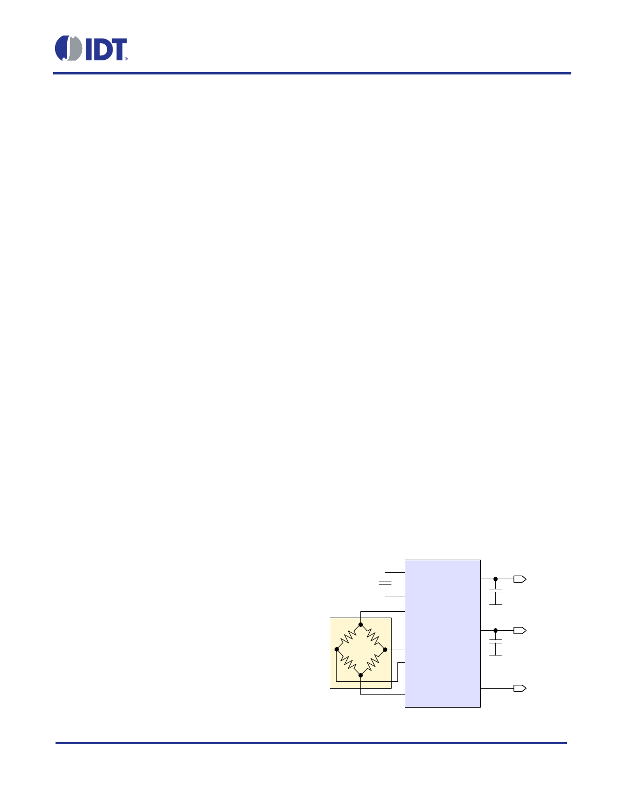
ZSSC3136 Minimum Application Requirements
Sensor
Module
VCC
ZSSC3136
OUT
GND
1 January 22, 2016
1 page 
ZSSC3136 Datasheet
1 Electrical Characteristics
1.1. Absolute Maximum Ratings
Parameters apply in operation temperature range and without time limitations.
Table 1.1 Absolute Maximum Ratings
No.
1.1.1
Parameter
Supply voltage 1)
1.1.2
1.1.3
Potential at AOUT pin 1)
Analog supply voltage 1)
Symbol
VDDEAMR
VOUT
VDDAAMR
Conditions
To VSSE, refer to
section 3 for application
circuits
Referenced to VSSE
Referenced to VSSA,
VDDE - VDDA < 0.35V
Min
-33
-33
-0.3
1.1.4
1.1.5
Voltage at all analog and
digital IO pins
Storage temperature
VA_IO
VD_IO
TSTG
Referenced to VSSA
-0.3
-55
1) Refer to the ZSSC313x Technical Note—High Voltage Protection for specification and detailed conditions.
Max Unit
33 VDC
33 VDC
6.5 VDC
VDDA + 0.3 VDC
150 °C
1.2. Operating Conditions
All voltages are referenced to VSSA.
Table 1.2 Operating Conditions
No.
1.2.1
Parameter
Ambient temperature 1) 2)
Symbol
TAMB_TQE
Conditions
Extended Temperature
Range (TQE)
Min Typ Max Unit
-40 150 °C
TAMB_TQA
Advanced-Performance
Temperature Range
(TQA)
-40
125 °C
TAMB_TQI
Best-Performance
Temperature Range (TQI)
-25
85 °C
1.2.2
1.2.3
Supply voltage
Bridge resistance 3) 4)
VDDE
RBR
4.5 5.0 5.5 VDC
2 25 kΩ
1) Maximum operation temperature range depends on product version (refer to section 8).
2) See the temperature profile description in the ZSSC313x Technical Note Die & Package Dimensions.
3) No measurement in mass production, parameter is guaranteed by design and/or quality observation.
4) Symmetric behavior and identical electrical properties (especially the low pass characteristic) of both sensor inputs of the ZSSC3136 are required.
Unsymmetrical conditions of the sensor and/or external components connected to the sensor input pins of the ZSSC3136can generate a failure in
signal operation.
© 2016 Integrated Device Technology, Inc.
5
January 22, 2016
5 Page 
ZSSC3136 Datasheet
The digital signal conditioning is processed by the calibration microcontroller (CMC). It is based on a correction
formula that uses sensor-specific coefficients determined during calibration. The formula is located in ROM, and
the sensor-specific coefficients are stored in EEPROM. Depending on the programmed output configuration, the
conditioned sensor signal is output as an analog signal, or alternatively can be readout via a digital serial interface
(I²C™ or ZACwire™). The configuration data and the correction parameters must also be programmed into the
EEPROM via the digital interfaces.
2.2. Application Modes
For each application, a configuration set must be established by programming the on-chip EEPROM for the
following modes:
• Sensor channel
Input range: The gain adjustment of the analog front-end (AFE) with respect to the maximum sensor
signal span and the zero point of the A/D conversion must be selected.
Resolution/response time: The A/D converter must be configured for resolution. These settings influence
the sampling rate and the signal integration time, and thus, the noise immunity.
• Temperature
Temperature measurement: Select the internal or external temperature sensor.
2.3. Analog Front-End (AFE)
The analog front-end (AFE) consists of the three-stage programmable gain amplifier (PGA), the multiplexer
(MUX), and the analog-to-digital converter (ADC).
2.3.1. Programmable Gain Amplifier (PGA)
Table 2.1 shows the adjustable gains, the sensor signal spans, and the valid common mode range.
Table 2.1 Adjustable Gains, Resulting Sensor Signal Spans and Common Mode Ranges
PGA Gain
aIN
105
Maximum Span
VIN_SP [mV/V] 1)
7.1
Input Common Mode Range
VIN_CM [% VDDA]
29 to 65
70 10.7 29 to 65
52.5 14.3 29 to 65
35 21.4 29 to 65
26.3 28.5 29 to 65
14
53.75
29 to 65
9.3 80 29 to 65
7 107 29 to 65
2.8 267 32 to 57
1) Recommended maximum internal signal range is 75% of supply voltage.
Span is calculated by the following formula: Span = 0.75 (VBR_T – VBR_B) / Gain.
© 2016 Integrated Device Technology, Inc.
11
January 22, 2016
11 Page | ||
| Páginas | Total 24 Páginas | |
| PDF Descargar | [ Datasheet ZSSC3136.PDF ] | |
Hoja de datos destacado
| Número de pieza | Descripción | Fabricantes |
| ZSSC3131 | Sensor Signal Conditioner | IDT |
| ZSSC3135 | Sensor Signal Conditioner | IDT |
| ZSSC3136 | Sensor Signal Conditioner | IDT |
| ZSSC3138 | Sensor Signal Conditioner | IDT |
| Número de pieza | Descripción | Fabricantes |
| SLA6805M | High Voltage 3 phase Motor Driver IC. |
Sanken |
| SDC1742 | 12- and 14-Bit Hybrid Synchro / Resolver-to-Digital Converters. |
Analog Devices |
|
DataSheet.es es una pagina web que funciona como un repositorio de manuales o hoja de datos de muchos de los productos más populares, |
| DataSheet.es | 2020 | Privacy Policy | Contacto | Buscar |