|
|
PDF CY7C1370KV25 Data sheet ( Hoja de datos )
| Número de pieza | CY7C1370KV25 | |
| Descripción | 18-Mbit (512K x 36/1M x 18) Pipelined SRAM | |
| Fabricantes | Cypress Semiconductor | |
| Logotipo | ||
Hay una vista previa y un enlace de descarga de CY7C1370KV25 (archivo pdf) en la parte inferior de esta página. Total 30 Páginas | ||
|
No Preview Available !
CY7C1370KV25
CY7C1372KV25
18-Mbit (512K × 36/1M × 18)
Pipelined SRAM with NoBL™ Architecture
18-Mbit (512K × 36/1M × 18) Pipelined SRAM with NoBL™ Architecture
Features
■ Pin-compatible and functionally equivalent to ZBT™
■ Supports 200-MHz bus operations with zero wait states
❐ Available speed grades are 200 and 167 MHz
■ Internally self-timed output buffer control to eliminate the need
to use asynchronous OE
■ Fully registered (inputs and outputs) for pipelined operation
■ Byte write capability
■ Single 2.5 V core power supply (VDD)
■ 2.5 V I/O power supply (VDDQ)
■ Fast clock-to-output times
❐ 3.2 ns (for 200-MHz device)
■ Clock enable (CEN) pin to suspend operation
■ Synchronous self-timed writes
■ Available in JEDEC-standard Pb-free 100-pin TQFP, and non
Pb-free 165-ball FBGA packages
■ IEEE 1149.1 JTAG-compatible boundary scan
■ Burst capability – linear or interleaved burst order
■ “ZZ” sleep mode option and stop clock option
Functional Description
The CY7C1370KV25 and CY7C1372KV25 are 2.5 V, 512K × 36
and 1M × 18 synchronous pipelined burst SRAMs with No Bus
Latency™ (NoBL™) logic, respectively. They are designed to
support unlimited true back-to-back read/write operations with
no wait states. The CY7C1370KV25 and CY7C1372KV25 are
equipped with the advanced NoBL logic required to enable
consecutive read/write operations with data being transferred on
every clock cycle. This feature dramatically improves the
throughput of data in systems that require frequent write/read
transitions. The CY7C1370KV25 and CY7C1372KV25 are
pin-compatible and functionally equivalent to ZBT devices.
All synchronous inputs pass through input registers controlled by
the rising edge of the clock. All data outputs pass through output
registers controlled by the rising edge of the clock. The clock
input is qualified by the clock enable (CEN) signal, which when
deasserted suspends operation and extends the previous clock
cycle.
Write operations are controlled by the byte write selects
(BWa–BWd for CY7C1370KV25 and BWa–BWb for
CY7C1372KV25) and a write enable (WE) input. All writes are
conducted with on-chip synchronous self-timed write circuitry.
Three synchronous chip enables (CE1, CE2, CE3) and an
asynchronous output enable (OE) provide for easy bank
selection and output three-state control. In order to avoid bus
contention, the output drivers are synchronously three-stated
during the data portion of a write sequence.
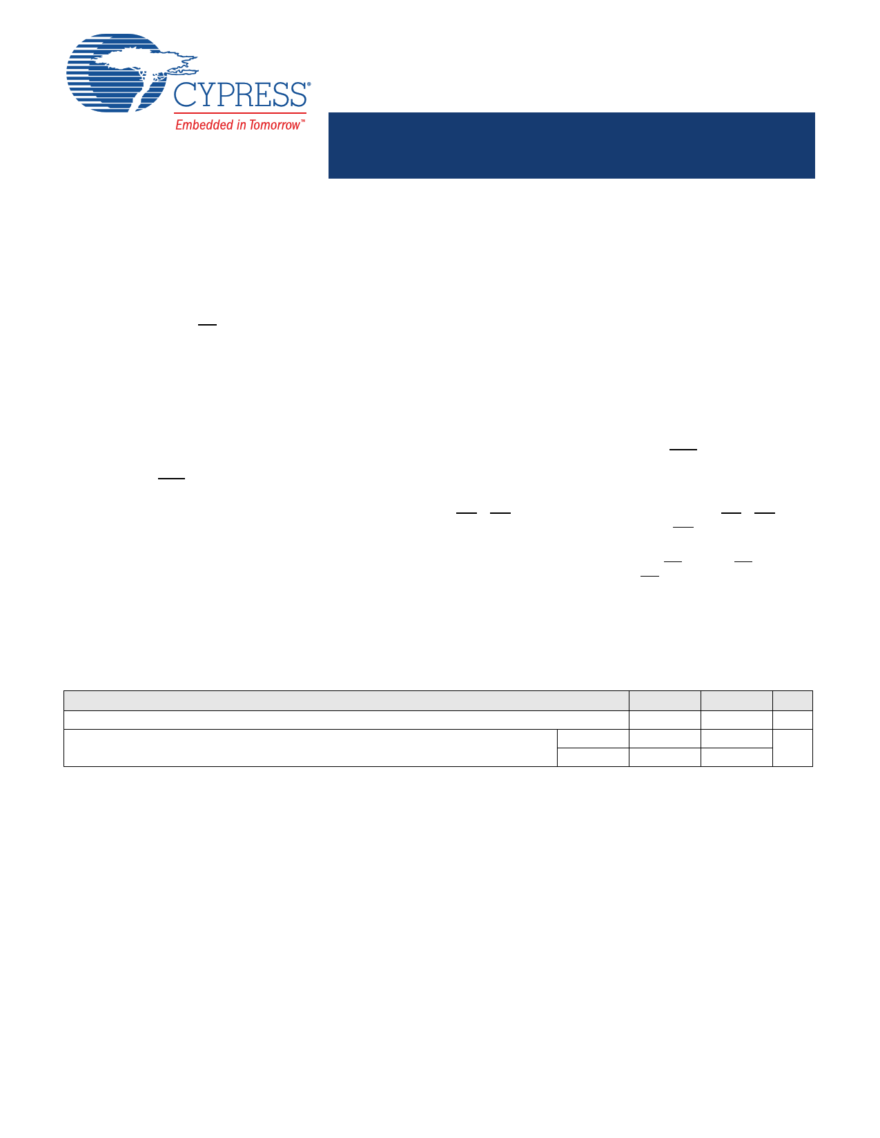
Selection Guide
Maximum access time
Maximum operating current
Description
× 18
× 36
200 MHz
3.0
158
178
167 MHz
3.4
143
163
Unit
ns
mA
Cypress Semiconductor Corporation • 198 Champion Court
Document Number: 001-97851 Rev. *F
• San Jose, CA 95134-1709 • 408-943-2600
Revised May 26, 2016
1 page 
CY7C1370KV25
CY7C1372KV25
Pin Configurations (continued)
Figure 2. 165-ball FBGA (13 × 15 × 1.4 mm) pinout, CY7C1370KV25 (512K x 36)
123
A NC/288M
B NC/144M
A
A
CE1
CE2
C DQPC NC VDDQ
D
DQC
DQC
VDDQ
E
DQC
DQC
VDDQ
F
DQC
DQC
VDDQ
G
DQC
DQC
VDDQ
H NC NC NC
J
DQD
DQD
VDDQ
K
DQD
DQD
VDDQ
L
DQD
DQD
VDDQ
M
DQD
DQD
VDDQ
N DQPD NC VDDQ
P NC NC/72M A
R MODE NC/36M A
4
BWC
BWD
VSS
VDD
VDD
VDD
VDD
VDD
VDD
VDD
VDD
VDD
VSS
A
A
5
BWB
BWA
VSS
VSS
VSS
VSS
VSS
VSS
VSS
VSS
VSS
VSS
NC
TDI
TMS
6
CE3
CLK
VSS
VSS
VSS
VSS
VSS
VSS
VSS
VSS
VSS
VSS
A
A1
A0
7
BWE
GW
VSS
VSS
VSS
VSS
VSS
VSS
VSS
VSS
VSS
VSS
NC
TDO
TCK
8
ADSC
OE
VSS
VDD
VDD
VDD
VDD
VDD
VDD
VDD
VDD
VDD
VSS
A
A
9
ADV
ADSP
VDDQ
VDDQ
VDDQ
VDDQ
VDDQ
NC
VDDQ
VDDQ
VDDQ
VDDQ
VDDQ
A
A
10 11
A NC
A NC/576M
NC/1G
DQB
DQPB
DQB
DQB
DQB
DQB
NC
DQB
DQB
DQB
ZZ
DQA
DQA
DQA
DQA
NC
A
DQA
DQA
DQA
DQA
DQPA
A
AA
Document Number: 001-97851 Rev. *F
Page 5 of 31
5 Page 
CY7C1370KV25
CY7C1372KV25
Partial Truth Table for Read/Write
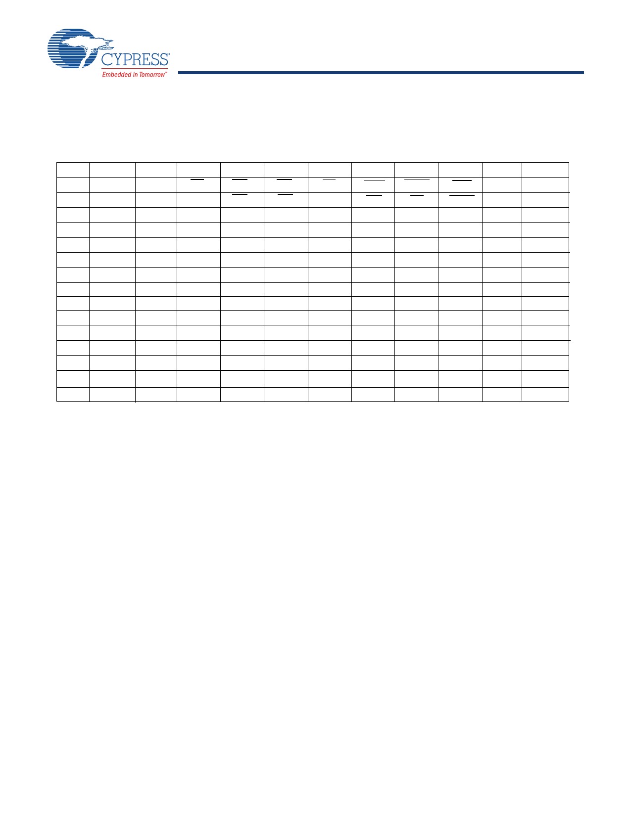
The partial truth table for Read/Write for CY7C1370KV25 follows. [9, 10, 11, 12]
Function (CY7C1370KV25)
WE
Read
Write – No bytes written
H
L
Write byte a – (DQa and DQPa)
Write byte b – (DQb and DQPb)
Write bytes b, a
Write byte c – (DQc and DQPc)
Write bytes c, a
Write bytes c, b
Write bytes c, b, a
L
L
L
L
L
L
L
Write byte d – (DQd and DQPd)
Write bytes d, a
L
L
Write bytes d, b
Write bytes d, b, a
Write bytes d, c
Write bytes d, c, a
Write bytes d, c, b
Write all bytes
L
L
L
L
L
L
Partial Truth Table for Read/Write
The partial truth table for Read/Write for CY7C1372KV25 follows. [9, 10, 11, 12]
Read
Function (CY7C1372KV25)
WE
H
Write – no bytes written
Write byte a – (DQa and DQPa)
Write byte b – (DQb and DQPb)
Write both bytes
L
L
L
L
BWd
X
H
H
H
H
H
H
H
H
L
L
L
L
L
L
L
L
BWc
X
H
H
H
H
L
L
L
L
H
H
H
H
L
L
L
L
BWb
x
H
H
L
L
BWb
X
H
H
L
L
H
H
L
L
H
H
L
L
H
H
L
L
BWa
X
H
L
H
L
H
L
H
L
H
L
H
L
H
L
H
L
BWa
x
H
L
H
L
Notes
9.
X=
that
“Don't Care”, H =
the desired byte
Logic HIGH,
write selects
L = Logic LOW, CE stands for all chip enables active. BWx =
are asserted, see Write Cycle Description table for details.
L
signifies
at
least
one
byte
write
select
is
active,
BWx
=
valid
signifies
10. Write is defined by WE and BWX. See Truth Table on page 10 for details.
11. When a write cycle is detected, all I/Os are tri-stated, even during byte writes.
12. Table only lists a partial listing of the byte write combinations. Any Combination of BWX is valid. Appropriate write will be done based on which byte write is active.
Document Number: 001-97851 Rev. *F
Page 11 of 31
11 Page | ||
| Páginas | Total 30 Páginas | |
| PDF Descargar | [ Datasheet CY7C1370KV25.PDF ] | |
Hoja de datos destacado
| Número de pieza | Descripción | Fabricantes |
| CY7C1370KV25 | 18-Mbit (512K x 36/1M x 18) Pipelined SRAM | Cypress Semiconductor |
| Número de pieza | Descripción | Fabricantes |
| SLA6805M | High Voltage 3 phase Motor Driver IC. |
Sanken |
| SDC1742 | 12- and 14-Bit Hybrid Synchro / Resolver-to-Digital Converters. |
Analog Devices |
|
DataSheet.es es una pagina web que funciona como un repositorio de manuales o hoja de datos de muchos de los productos más populares, |
| DataSheet.es | 2020 | Privacy Policy | Contacto | Buscar |
