|
|
PDF CY7C13451G Data sheet ( Hoja de datos )
| Número de pieza | CY7C13451G | |
| Descripción | 4-Mbit Flow-Through Sync SRAM | |
| Fabricantes | Cypress Semiconductor | |
| Logotipo | ||
Hay una vista previa y un enlace de descarga de CY7C13451G (archivo pdf) en la parte inferior de esta página. Total 23 Páginas | ||
|
No Preview Available !
CY7C13451G
4-Mbit (128K × 36) Flow-Through
Sync SRAM
4-Mbit (128K × 36) Flow-Through Sync SRAM
Features
■ 128K × 36 common I/O
■ 3.3 V core Power Supply (VDD)
■ 2.5 V or 3.3 V I/O Supply (VDDQ)
■ Fast Clock-to-output times
❐ 8.0 ns (100 MHz version)
■ Provide high performance 2-1-1-1 access rate
■ User selectable burst counter supporting Intel Pentium
interleaved or Linear Burst Sequences
■ Separate Processor and Controller Address Strobes
■ Synchronous Self Timed Write
■ Asynchronous output enable
■ Available in Pb-free 165-ball FBGA Package
■ ZZ Sleep Mode option
Selection Guide
Maximum Access Time
Maximum Operating Current
Maximum CMOS Standby Current
Description
Functional Description
The CY7C13451G is a 128K × 36 synchronous cache RAM
designed to interface with high speed microprocessors with
minimum glue logic. The maximum access delay from clock rise
is 8.0 ns (100 MHz version). A 2 bit on-chip counter captures the
first address in a burst and increments the address automatically
for the rest of the burst access. All synchronous inputs are gated
by registers controlled by a positive edge triggered Clock Input
(CLK). The synchronous inputs include all addresses, all data
inputs, address pipelining Chip Enable (CE1), depth expansion
Chip Enables (CE2 and CE3), Burst Control inputs (ADSC,
ADSP, and ADV), Write Enables (BWx, and BWE), and Global
Write (GW). Asynchronous inputs include the Output Enable
(OE) and the ZZ pin.
The CY7C13451G enables either interleaved or linear burst
sequences, selected by the MODE input pin. A HIGH selects an
interleaved burst sequence, while a LOW selects a linear burst
sequence. Burst accesses are initiated with the Processor
Address Strobe (ADSP) or the cache Controller Address Strobe
(ADSC) inputs.
Addresses and chip enables are registered at rising edge of
clock when either Address Strobe Processor (ADSP) or Address
Strobe Controller (ADSC) is active. Subsequent burst addresses
are internally generated as controlled by the Advance pin (ADV).
The CY7C13451G operates from a +3.3 V core power supply
while all outputs operate with either a +2.5 or +3.3 V supply. All
inputs and outputs are JEDEC standard JESD8-5 compatible.
For a complete list of related documentation, click here.
100 MHz
8.0
180
60
Unit
ns
mA
mA
Cypress Semiconductor Corporation • 198 Champion Court
Document Number: 001-88572 Rev. *F
• San Jose, CA 95134-1709 • 408-943-2600
Revised June 29, 2016
1 page 
CY7C13451G
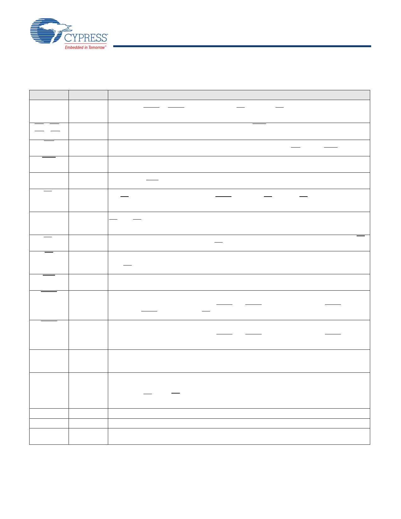
Pin Definitions
Name
I/O
Description
A0, A1, A
Input- Address Inputs Used to Select One of the 128K Address Locations. Sampled at the rising edge
Synchronous of the CLK if ADSP or ADSC is active LOW, and CE1, CE2, and CE3 are sampled active. A[1:0] feed
the two bit counter.
BWA, BWB,
BWC, BWD
GW
BWE
Input- Byte Write Select Inputs, Active LOW. Qualified with BWE to conduct byte writes to the SRAM.
Synchronous Sampled on the rising edge of CLK.
Input- Global Write Enable Input, Active LOW. When asserted LOW on the rising edge of CLK, a global
Synchronous write is conducted (ALL bytes are written, regardless of the values on BW[A:D] and BWE).
Input- Byte Write Enable Input, Active LOW. Sampled on the rising edge of CLK. This signal is asserted
Synchronous LOW to conduct a byte write.
CLK Input Clock Clock Input. Used to capture all synchronous inputs to the device. Also used to increment the burst
counter when ADV is asserted LOW, during a burst operation.
CE1
Input- Chip Enable 1 Input, Active LOW. Sampled on the rising edge of CLK. Used in conjunction with CE2
Synchronous and CE3 to select or deselect the device. ADSP is ignored if CE1 is HIGH. CE1 is sampled only when
a new external address is loaded.
CE2 Input- Chip Enable 2 Input, Active HIGH. Sampled on the rising edge of CLK. Used in conjunction with
Synchronous CE1 and CE3 to select or deselect the device. CE2 is sampled only when a new external address is
loaded.
CE3
Input- Chip Enable 3 Input, Active LOW. Sampled on the rising edge of CLK. Used in conjunction with CE1
Synchronous and CE2 to select or deselect the device. CE3 is sampled only when a new external address is loaded.
OE Input- Output Enable, Asynchronous Input, Active LOW. Controls the direction of the I/O pins. When
Asynchronou LOW, the I/O pins act as outputs. When deasserted HIGH, I/O pins are tristated and act as input data
s pins. OE is masked during the first clock of a read cycle when emerging from a deselected state.
ADV
Input- Advance Input Signal, Sampled on the Rising Edge of CLK. When asserted, it automatically incre-
Synchronous ments the address in a burst cycle.
ADSP
ADSC
ZZ [2]
Input- Address Strobe from Processor, Sampled on the Rising Edge of CLK, Active LOW. When
Synchronous asserted LOW, addresses presented to the device are captured in the address registers. A[1:0] are
also loaded into the burst counter. When ADSP and ADSC are both asserted, only ADSP is
recognized. ASDP is ignored when CE1 is deasserted HIGH.
Input- Address Strobe from Controller, Sampled on the Rising Edge of CLK, Active LOW. When
Synchronous asserted LOW, addresses presented to the device are captured in the address registers. A[1:0] are
also loaded into the burst counter. When ADSP and ADSC are both asserted, only ADSP is recog-
nized.
Input- ZZ sleep Input, Active HIGH. When asserted HIGH places the device in a non-time critical sleep
Asynchronou condition with data integrity preserved. During normal operation, this pin is low or left floating. ZZ pin
s has an internal pull down.
DQs, DQPA,
I/O- Bidirectional Data I/O lines. As inputs, they feed into an on-chip data register that is triggered by the
DQPB, DQPC, Synchronous rising edge of CLK. As outputs, they deliver the data contained in the memory location specified by
DQPD
the addresses presented during the previous clock rise of the read cycle. The direction of the pins is
controlled by OE. When OE is asserted LOW, the pins act as outputs. When HIGH, DQs and DQP[A:D]
are placed in a tristate condition.
VDD
VSS
VDDQ
Power Supply Power Supply Inputs to the Core of the Device.
Ground Ground for the Core of the Device.
I/O Power Power Supply for the I/O Circuitry.
Supply
Note
2. Errata: The ZZ pin (Ball H11) needs to be externally connected to ground. For more information, see “Errata” on page 21.
Document Number: 001-88572 Rev. *F
Page 5 of 23
5 Page 
CY7C13451G
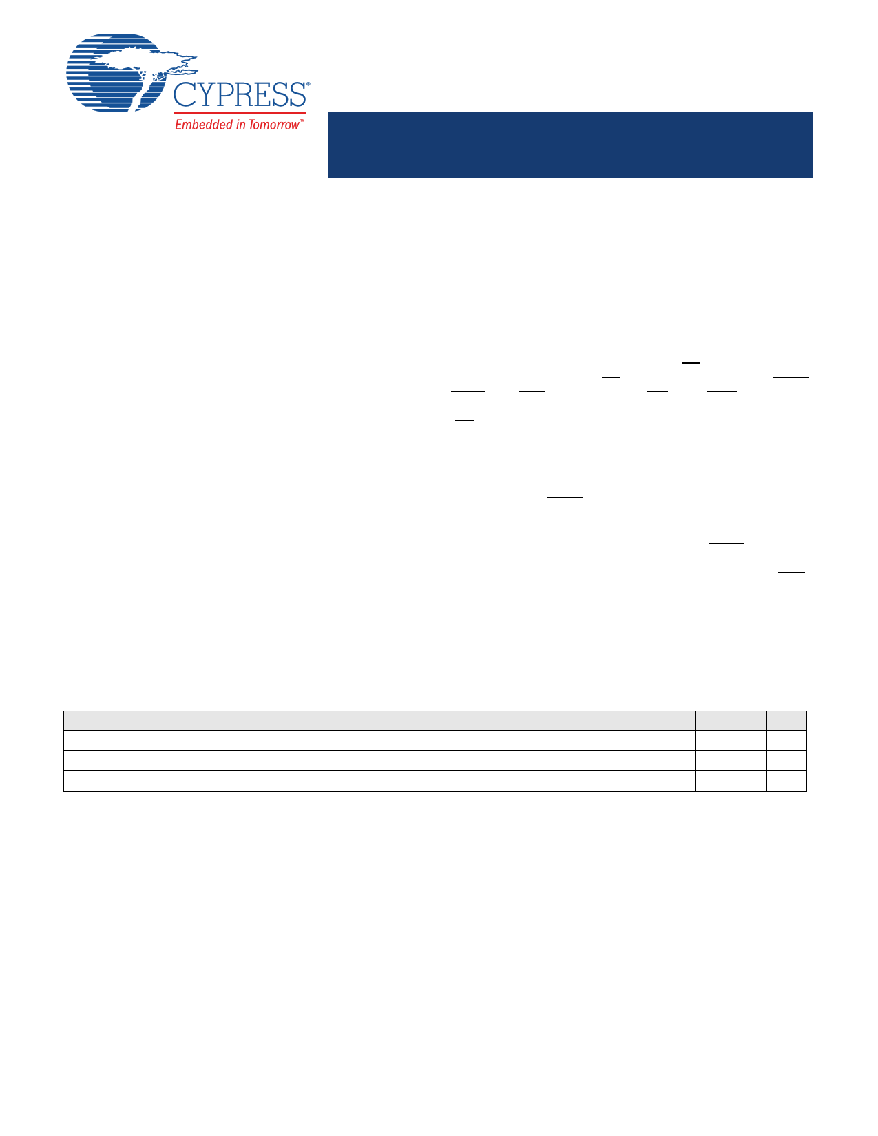
Electrical Characteristics (continued)
Over the Operating Range
Parameter [10, 11]
Description
IDD VDD Operating Supply Current
ISB1 Automatic CE Power-down
Current – TTL Inputs
ISB2 Automatic CE Power-down
Current – CMOS Inputs
ISB3 Automatic CE Power-down
Current – CMOS Inputs
ISB4 Automatic CE Power-down
Current – TTL Inputs
Test Conditions
VDD = Max., IOUT = 0 mA,
f = fMAX = 1/tCYC
Max. VDD, Device Deselected,
VIN> VIH or VIN < VIL, f = fMAX,
inputs switching
100 MHz
100 MHz
(Automotive)
Max. VDD, Device Deselected, 100 MHz
VIN > VDD – 0.3 V or VIN < 0.3 V, (Automotive)
f = 0, inputs static
Max. VDD, Device Deselected, 100 MHz
VIN > VDDQ – 0.3 V or VIN < 0.3 V, (Automotive)
f = fMAX, inputs switching
Max. VDD, Device Deselected,
VIN > VIH or VIN < VIL,
f = 0, inputs static
100 MHz
(Automotive)
Min
–
–
–
–
–
Max Unit
180 mA
150 mA
40 mA
120 mA
60 mA
Capacitance
Parameter [12]
Description
CIN
CCLK
CI/O
Input capacitance
Clock input capacitance
Input/Output capacitance
Thermal Resistance
Parameter [12]
Description
JA Thermal resistance
(junction to ambient)
JC Thermal resistance
(junction to case)
Test Conditions
TA = 25 C, f = 1 MHz,
VDD = 3.3 V, VDDQ = 2.5 V
165-ball FBGA
Max.
Unit
5 pF
5 pF
7 pF
Test Conditions
165-ball FBGA
Package
Unit
Test conditions follow standard test methods and
procedures for measuring thermal impedance, per
EIA/JESD51.
16.8
3.0
°C/W
°C/W
Note
12. Tested initially and after any design or process change that may affect these parameters.
Document Number: 001-88572 Rev. *F
Page 11 of 23
11 Page | ||
| Páginas | Total 23 Páginas | |
| PDF Descargar | [ Datasheet CY7C13451G.PDF ] | |
Hoja de datos destacado
| Número de pieza | Descripción | Fabricantes |
| CY7C13451G | 4-Mbit Flow-Through Sync SRAM | Cypress Semiconductor |
| Número de pieza | Descripción | Fabricantes |
| SLA6805M | High Voltage 3 phase Motor Driver IC. |
Sanken |
| SDC1742 | 12- and 14-Bit Hybrid Synchro / Resolver-to-Digital Converters. |
Analog Devices |
|
DataSheet.es es una pagina web que funciona como un repositorio de manuales o hoja de datos de muchos de los productos más populares, |
| DataSheet.es | 2020 | Privacy Policy | Contacto | Buscar |
