|
|
|
PDF CY14B101LA Data sheet ( Hoja de datos )
| Número de pieza | CY14B101LA | |
| Descripción | 1-Mbit (128 K x 8/64 K x 16) nvSRAM | |
| Fabricantes | Cypress Semiconductor | |
| Logotipo | ||
Hay una vista previa y un enlace de descarga de CY14B101LA (archivo pdf) en la parte inferior de esta página. Total 30 Páginas | ||
|
No Preview Available !
CY14B101LA
CY14B101NA
1-Mbit (128 K × 8/64 K × 16) nvSRAM
1-Mbit (128 K × 8/64 K × 16) nvSRAM
Features
■ 20 ns, 25 ns, and 45 ns access times
■ Internally organized as 128 K × 8 (CY14B101LA) or 64 K × 16
(CY14B101NA)
■ Hands off automatic STORE on power-down with only a small
capacitor
■ STORE to QuantumTrap nonvolatile elements initiated by
software, device pin, or AutoStore on power-down
■ RECALL to SRAM initiated by software or power-up
■ Infinite read, write, and RECALL cycles
■ 1 million STORE cycles to QuantumTrap
■ 20 year data retention
■ Single 3 V +20% to –10% operation
■ Industrial temperature
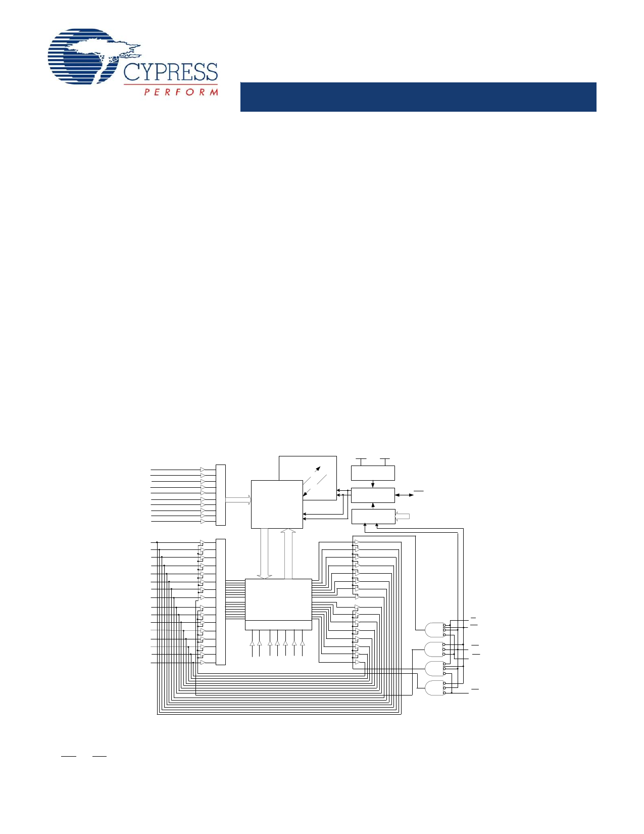
Logic Block Diagram [1, 2, 3]
■ Packages
❐ 32-pin small-outline integrated circuit (SOIC)
❐ 44-/54-pin thin small outline package (TSOP) Type II
❐ 48-pin shrink small-outline package (SSOP)
❐ 48-ball fine-pitch ball grid array (FBGA)
■ Pb-free and restriction of hazardous substances (RoHS)
compliant
Functional Description
The Cypress CY14B101LA/CY14B101NA is a fast static RAM
(SRAM), with a nonvolatile element in each memory cell. The
memory is organized as 128 K bytes of 8 bits each or 64 K words
of 16 bits each. The embedded nonvolatile elements incorporate
QuantumTrap technology, producing the world’s most reliable
nonvolatile memory. The SRAM provides infinite read and write
cycles, while independent nonvolatile data resides in the highly
reliable QuantumTrap cell. Data transfers from the SRAM to the
nonvolatile elements (the STORE operation) takes place
automatically at power-down. On power-up, data is restored to
the SRAM (the RECALL operation) from the nonvolatile memory.
Both the STORE and RECALL operations are also available
under software control.
For a complete list of related resources, click here.
Quatrum Trap
VCC
VCAP
1024 X 1024
A5
R
O
A6 W
STORE
POWER
CONTROL
A7
A8
A9
A12
RECALL
D
E
C STATIC RAM
STORE/RECALL
CONTROL
HSB
A13 O ARRAY
A14
A15
A16
D 1024 X 1024
E
R
SOFTWARE
DETECT
A14 - A2
DQ0
DQ1
DQ2
DQ3
DQ4
DQ5
DQ6
DQ7
DQ8
DQ9
DQ10
DQ11
DQ12
DQ13
DQ14
DQ15
I
N
P
U
T
B COLUMN I/O
U
F
F
E
R COLUMN DEC
S
A0 A1 A2 A3 A4 A10 A11
OE
WE
CE
BLE
BHE
Notes
1. Address A0–A16 for × 8 configuration and Address A0–A15 for × 16 configuration.
2. Data DQ0–DQ7 for × 8 configuration and Data DQ0–DQ15 for × 16 configuration.
3. BHE and BLE are applicable for × 16 configuration only.
Cypress Semiconductor Corporation • 198 Champion Court
Document Number: 001-42879 Rev. *Q
• San Jose, CA 95134-1709 • 408-943-2600
Revised November 12, 2014
1 page 
CY14B101LA
CY14B101NA
Pin Definitions
Pin Name I/O Type
Description
A0–A16
A0–A15
DQ0–DQ7
DQ0–DQ15
WE
Input
Input/Output
Input
Address inputs. Used to select one of the 131,072 bytes of the nvSRAM for × 8 configuration.
Address inputs. Used to select one of the 65,536 words of the nvSRAM for × 16 configuration.
Bidirectional data I/O lines for × 8 configuration. Used as input or output lines depending on operation.
Bidirectional Data I/O Lines for × 16 configuration. Used as input or output lines depending on operation.
Write Enable input, Active LOW. When the chip is enabled and WE is LOW, data on the I/O pins is written
to the specific address location.
CE Input Chip Enable input, Active LOW. When LOW, selects the chip. When HIGH, deselects the chip.
OE Input Output Enable, Active LOW. The active LOW OE input enables the data output buffers during read cycles.
I/O pins are tristated on deasserting OE HIGH.
BHE
BLE
VSS
VCC
HSB[13]
Input
Input
Ground
Byte High Enable, Active LOW. Controls DQ15–DQ8.
Byte Low Enable, Active LOW. Controls DQ7–DQ0.
Ground for the device. Must be connected to the ground of the system.
Power supply Power supply inputs to the device. 3.0 V +20%, –10%
Input/Output Hardware STORE Busy (HSB). When LOW, this output indicates that a Hardware STORE is in progress.
When pulled LOW, external to the chip, it initiates a nonvolatile STORE operation. After each Hardware
and Software STORE operation HSB is driven HIGH for a short time (tHHHD) with standard output high
current and then a weak internal pull-up resistor keeps this pin HIGH (external pull-up resistor connection
optional).
VCAP Power supply AutoStore capacitor. Supplies power to the nvSRAM during power loss to store data from SRAM to
nonvolatile elements.
NC No connect No connect. This pin is not connected to the die.
Note
13. HSB pin is not available in 44-pin TSOP II (× 16) package.
Document Number: 001-42879 Rev. *Q
Page 5 of 30
5 Page 
CY14B101LA
CY14B101NA
AC Test Loads
3.0 V
OUTPUT
30 pF
577
R1
Figure 5. AC Test Loads
R2
789
3.0 V
OUTPUT
5 pF
AC Test Conditions
Input pulse levels ...................................................0 V to 3 V
Input rise and fall times (10%–90%) ........................... < 3 ns
Input and output timing reference levels ....................... 1.5 V
577
R1
for tristate specs
R2
789
Document Number: 001-42879 Rev. *Q
Page 11 of 30
11 Page | ||
| Páginas | Total 30 Páginas | |
| PDF Descargar | [ Datasheet CY14B101LA.PDF ] | |
Hoja de datos destacado
| Número de pieza | Descripción | Fabricantes |
| CY14B101L | 1-Mbit (128K x 8) nvSRAM | Cypress Semiconductor |
| CY14B101LA | 1-Mbit (128 K x 8/64 K x 16) nvSRAM | Cypress Semiconductor |
| Número de pieza | Descripción | Fabricantes |
| SLA6805M | High Voltage 3 phase Motor Driver IC. |
Sanken |
| SDC1742 | 12- and 14-Bit Hybrid Synchro / Resolver-to-Digital Converters. |
Analog Devices |
|
DataSheet.es es una pagina web que funciona como un repositorio de manuales o hoja de datos de muchos de los productos más populares, |
| DataSheet.es | 2020 | Privacy Policy | Contacto | Buscar |