|
|
|
PDF A8510 Data sheet ( Hoja de datos )
| Número de pieza | A8510 | |
| Descripción | High Efficiency Fault Tolerant LED Driver | |
| Fabricantes | Allegro | |
| Logotipo | ||
Hay una vista previa y un enlace de descarga de A8510 (archivo pdf) en la parte inferior de esta página. Total 30 Páginas | ||
|
No Preview Available !
A8510
Wide Input Voltage Range, High Efficiency
Fault Tolerant LED Driver
Features and Benefits
• Integrated 2 MHz capable boost converter with 60 V DMOS
switch with OVP protection
• Sync function to synchronize boost converter switching
frequencies up to 2.3 MHz
• LED current up to 40 mA per LED channel into 8 channels
• Drives up to 12 series LEDs in 8 parallel strings
(Vf = 3.5 V, If = 40 mA), VIN = 8 V, switching frequency
of 1 MHz
• Single EN/PWM pin interface for PWM dimming and
enable functions
• APWM pin for fine-tuning color adjustment and/or
maximizing contrast ratio
• Integrated driver for optional external PMOS input
disconnect switch
• Typical LED accuracy of 0.7% and 0.8% for
LED-to-LED matching
• Internal bias supply for single-supply operation
from 5 to 40 V
• Extensive protection features
Package: 26-pin QFN (suffix EC)
Description
The A8510 is a multi-output white LED driver for LCD
backlighting. It integrates a current-mode boost converter with
internal power switch and 8 current sinks. The boost converter
can drive up to 96 LEDs with 12 LEDs at 40 mA per string.
The LED sinks can also be paralleled together to achieve even
higher LED currents, up to 320 mA. The A8510 can operate
from a single power supply, from 5 to 40 V.
If required, the A8510 can drive an external P-FET to
disconnect the input supply from the system in the event of a
fault. The A8510 provides protection against output short and
overvoltage, open or shorted diode, open or shorted LED pin,
and overtemperature. Adual level cycle-by-cycle current limit
function provides soft start and protects the internal current
switch against high current overloads.
The A8510 has a synchronization pin that allows PWM
switching frequencies to be synchronized in the range of
580 kHz to 2.3 MHz.
The device package is a 26-contact, 4 mm × 4 mm, 0.75 mm
nominal overall height QFN, with exposed pad for enhanced
thermal dissipation. It is lead (Pb) free, with 100% matte tin
leadframe plating.
Approximate scale 1:1
Applications
• Industrial LCD displays
• Backlighting LCD displays
• Infotainment displays
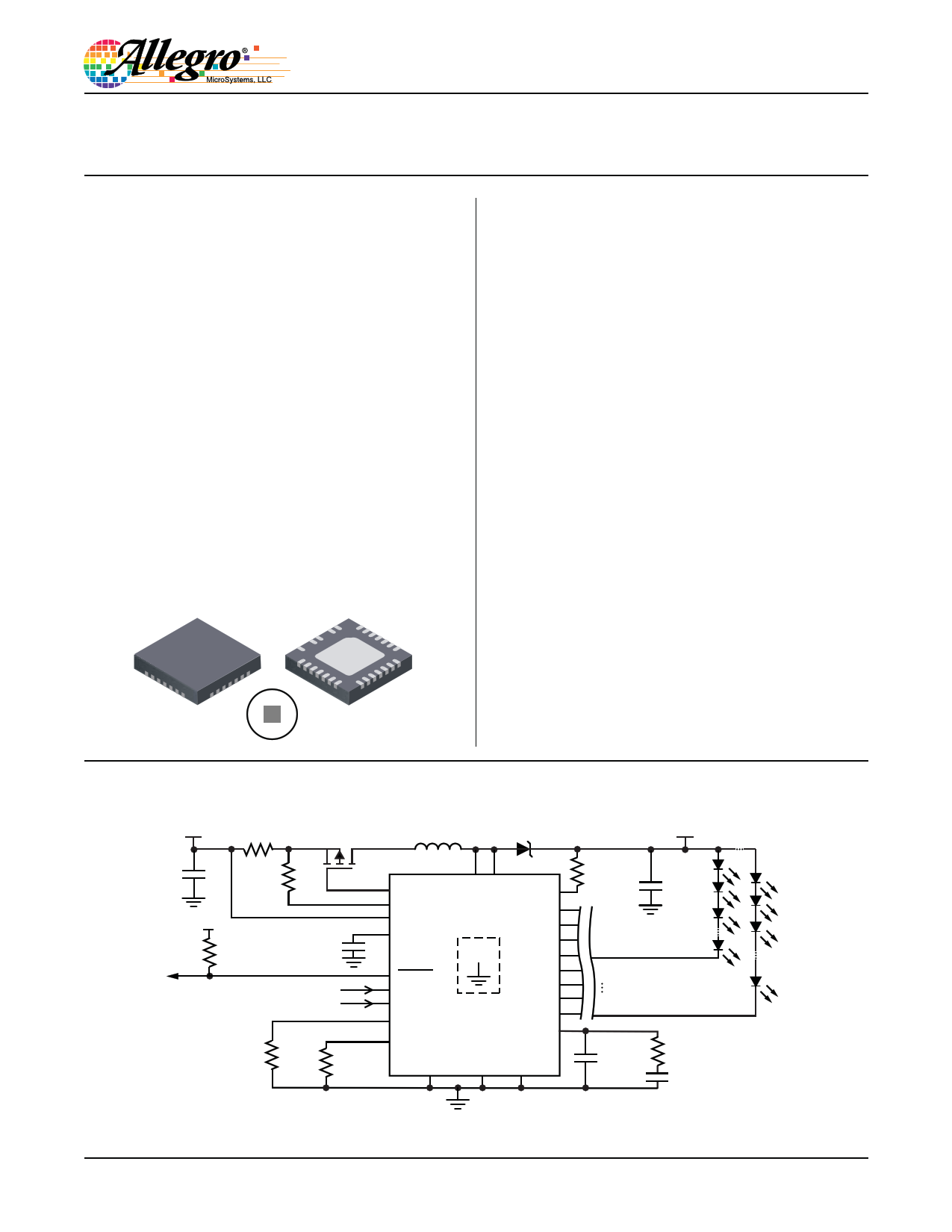
Typical Application Diagram
VIN
RSC
0.056 Ω
Q1
L1
22 μH
D1
2 A / 60 V
4.7 μCFI/N50 V
VC
100 kΩ
RADJ
590 Ω
RISET
8.25 kΩ
CVDD
0.1 μF
RFSET
25.5 kΩ
VGATE
VSENSE
VIN
VDD
SW SW
A8510
OVP
LED1
LED2
LED3
PAD LED4
FAULT
EN/PWM
APWM
ISET
FSET/SYNC
LED5
LED6
LED7
LED8
COMP
AGND PGND PGND
16R9OkVΩP
CP
120 pF
VOUT
COUT
4.7 μF
50 V
1R2Z0 Ω
0C.Z47 μF
Figure 1. Typical Application Circuit showing VIN to GND
short protection using P-MOSFET sensing
A8510-DS, Rev. 2
1 page 
A8510
Wide Input Voltage Range, High Efficiency
Fault Tolerant LED Driver
ELECTRICAL CHARACTERISTICS1 Valid at VIN = 16 V, TA = 25°C, indicates specifications guaranteed by design and
characterization over the full operating temperature range with TA = TJ = –40°C to 105°C; unless otherwise noted
Characteristics
Symbol
Test Conditions
Min.
Typ.2
Max.
Input Voltage Specifications
Operating Input Voltage Range3
VIN
5 – 40
UVLO Start Threshold
VUVLOrise VIN rising
− – 4.35
UVLO Stop Threshold
VUVLOfall VIN falling
− – 3.90
UVLO Hysteresis4
Input Currents
VUVLOhys
– 450 –
Input Quiescent Current
IQ EN/PWM = VIH ; SW = 2 MHz, no load
− 5.5 −
Input Sleep Supply Current
IQSLEEP
Input Logic Levels (EN/PWM, APWM)
VIN = 16 V, EN/PWM = SYNC = 0 V
− 2 10.0
Input Logic Level-Low
VIL VIN throughout operating input voltage range – – 400
Input Logic Level-High
EN/PWM Pin Pin Pull-Down Resistor
APWM Pin Pull-Down Resistor
APWM
VIH
REN
RAPWM
VIN throughout operating input voltage range
EN/PWM = 5 V
APWM = VIH
1.5 –
– 100
– 100
–
–
–
APWM Frequency
Error Amplifier
fAPWM
20 − 1000
Open Loop Voltage Gain
Transconductance
Source Current
Sink Current
COMP Pin Pull-Down Resistor
Overvoltage Protection
AVOL
gm
IEA(SRC)
IEA(SINK)
RCOMP
ΔICOMP = ±10 μA
VCOMP = 1.5 V
VCOMP = 1.5 V
− 48 −
− 990 −
− –350 −
− 350 −
− 2000 −
Overvoltage Threshold
VOVP(th) OVP connected to VOUT
7.7 8.1 8.5
OVP Sense Current
IOVPH
188 199 210
OVP Leakage Current
IOVPLKG ROVP = 40.2 kΩ, VIN = 16 V, EN/PWM = VIL
− 0.1 1
Secondary Overvoltage Protection
Boost Switch
VOVP(sec)
− 55 −
Switch On-Resistance
Switch Leakage Current
RSW
ISWLKG
ISW = 0.750 A, VIN = 16 V
VSW = 16 V, EN/PWM = VIL
− 300 −
− 0.1 1
Switch Current Limit
Secondary Switch Current Limit4
ISW(LIM)
ISW(LIM2)
Higher than ISW(LIM)(max) for all conditions,
device latches when detected
3.0 3.5 4.2
− 7.0 −
Soft Start Boost Current Limit
Minimum Switch On-Time
Minimum Switch Off-Time
ISWSS(LIM)
tSWONTIME
tSWOFFTIME
Initial soft start current for boost switch
− 700 −
− 85 −
− 47 −
Unit
V
V
V
mV
mA
μA
mV
V
kΩ
kΩ
kHz
dB
μA/V
μA
μA
Ω
V
μA
μA
V
mΩ
μA
A
A
mA
ns
ns
Continued on the next page…
Allegro MicroSystems, LLC
115 Northeast Cutoff
Worcester, Massachusetts 01615-0036 U.S.A.
1.508.853.5000; www.allegromicro.com
5
5 Page 
A8510
Wide Input Voltage Range, High Efficiency
Fault Tolerant LED Driver
All unused pins should be connected with a 4.75 kΩ resistor to
GND, as shown in figure 5. The unused pin, with the pull-down
resistor, will be taken out of regulation at this point and will not
contribute to the boost regulation loop.
If an LEDx pin is shorted to ground the A8510 will not proceed
with soft start until the short is removed from the LEDx pin. This
prevents the A8510 from powering-up and putting an uncon-
trolled amount of current through the LEDs. The various detect
scenarios are presented in figures 4A and 4B.
A8510
LED1
LED2
LED3
LED4
LED5
LED6
LED7
GND
LED8
4.75 kΩ
A8510
LED1
LED2
LED3
LED4
LED5
LED6
LED7
GND
LED8
Figure 5. Channel select setup: (left) channel LED8 not used,
(right) using all channels.
LED1-7
C1 LED detection period
C2
LED8
C3
ISET
C4 EN/PWM
t
4A. Example with LED8 pin not being used; fSW is 2 MHz, the detect voltage
is about 150 mV; shows LED1-7 (ch1, 500 mV/div.), LED8 (ch2, 500 mV/div.),
ISET (ch3, 1 V/div.), and EN/PWM (ch4, 5 V/div.) pins, t = 500 μs/div.
Pin shorted
C1
Short removed
LED1
LED2
C2
ISET
C3
C4 EN/PWM
t
4B. Example with one LED shorted to GND. The IC will not proceed with power-
up until the shorted LED pin is released, at which point the LED is checked to
see if it is being used; shows LED1 (ch1, 500 mV/div.), LED2 (ch2, 500 mV/div.),
ISET (ch3, 1 V/div.), and EN/PWM (ch4, 5 V/div.) pins, t = 1 ms/div.
.
Allegro MicroSystems, LLC
115 Northeast Cutoff
Worcester, Massachusetts 01615-0036 U.S.A.
1.508.853.5000; www.allegromicro.com
11
11 Page | ||
| Páginas | Total 30 Páginas | |
| PDF Descargar | [ Datasheet A8510.PDF ] | |
Hoja de datos destacado
| Número de pieza | Descripción | Fabricantes |
| A8510 | High Efficiency Fault Tolerant LED Driver | Allegro |
| A8512 | LED Backlight Driver | Allegro Micro Systems |
| A8514 | High Efficiency Fault Tolerant LED Driver | Allegro |
| Número de pieza | Descripción | Fabricantes |
| SLA6805M | High Voltage 3 phase Motor Driver IC. |
Sanken |
| SDC1742 | 12- and 14-Bit Hybrid Synchro / Resolver-to-Digital Converters. |
Analog Devices |
|
DataSheet.es es una pagina web que funciona como un repositorio de manuales o hoja de datos de muchos de los productos más populares, |
| DataSheet.es | 2020 | Privacy Policy | Contacto | Buscar |