|
|
|
PDF DG405 Data sheet ( Hoja de datos )
| Número de pieza | DG405 | |
| Descripción | Improved / Dual / High-Speed Analog Switches | |
| Fabricantes | Maxim Integrated | |
| Logotipo | ||
Hay una vista previa y un enlace de descarga de DG405 (archivo pdf) en la parte inferior de esta página. Total 8 Páginas | ||
|
No Preview Available !
19-4727; Rev 2; 6/99
Improved, Dual, High-Speed Analog Switches
_______________General Description ______________________New Features
Maxim's redesigned DG401/DG403/DG405 analog
switches now feature guaranteed low on-resistance
matching between switches (2Ω max) and guaranteed
on-resistance flatness over the signal range (3Ω max).
These low on-resistance switches (20Ω typ) conduct
equally well in either direction and are guaranteed to
have low charge injection (15pC max). The new design
offers lower off leakage current over temperature (less
than 5nA at +85°C).
The DG401/DG403/DG405 are dual, high-speed
switches. The single-pole/single-throw DG401 and
double-pole/single-throw DG405 are normally open
dual switches. The dual, single-pole/double-throw
DG403 has two normally open and two normally closed
switches. Switching times are 150ns max for tON and
100ns max for tOFF, with a maximum power consump-
tion of 35µW. These devices operate from a single
+10V to +30V supply, or bipolar supplies of ±4.5V to
±20V. Maxim's improved DG401/DG403/DG405 are
fabricated with a 44V silicon-gate process.
o Plug-In Upgrade for Industry-Standard
DG401/DG403/DG405
o Improved rDS(ON) Match Between Channels (2Ω max)
o Guaranteed rFLAT(ON) Over Signal Range (3Ω max)
o Improved Charge Injection (15pC max)
o Improved Off Leakage Current Over Temperature
(<5nA at +85°C)
__________________Existing Features
o Low rDS(ON) (30Ω max)
o Single-Supply Operation +10V to +30V
Bipolar-Supply Operation ±4.5V to ±20V
o Low Power Consumption (35µW max)
o Rail-to-Rail Signal Handling Capability
o TTL/CMOS-Logic Compatible
______________Ordering Information
________________________Applications
Sample-and-Hold Circuits
Test Equipment
Guidance and Control Systems Heads-Up Displays
PART
DG401CJ
DG401CY
TEMP. RANGE
0°C to +70°C
0°C to +70°C
PIN PACKAGE
16 Plastic DIP
16 Narrow SO
Communications Systems
PBX, PABX
DG401C/D
0°C to +70°C
Dice*
Battery-Operated Systems
Military Radios
Audio Signal Routing
Ordering Information continued on last page.
*Contact factory for dice specifications.
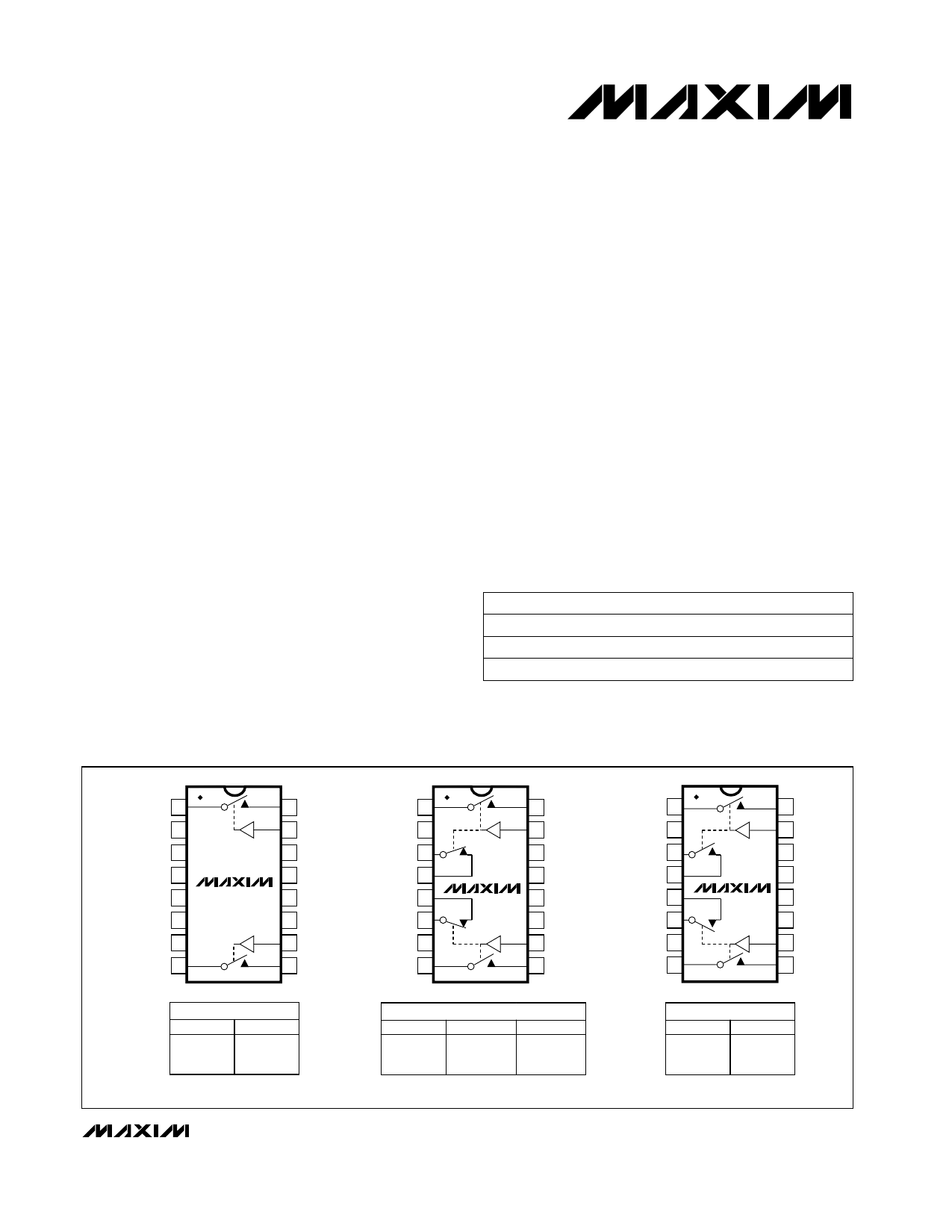
_____________________Pin Configurations/Functional Diagrams/Truth Tables
TOP VIEW
D1 1
N.C. 2
N.C. 3
N.C. 4
N.C. 5
N.C. 6
N.C. 7
D2 8
DG401
16 S1
15 IN1
14 V-
13 GND
12 VL
11 V+
10 IN2
9 S2
DIP/SO
DG401
LOGIC
SWITCH
0 OFF
1 ON
LCC packages on last page.
D1 1
N.C. 2
D3 3
S3 4
S4 5
D4 6
N.C. 7
D2 8
LOGIC
0
1
16 S1
15 IN1
14 V-
13 GND
DG403 12 VL
11 V+
10 IN2
9 S2
DIP/SO
DG403
SWITCHES 1, 2 SWITCHES 3, 4
OFF ON
ON OFF
SWITCHES SHOWN FOR LOGIC "0" INPUT
D1 1
N.C. 2
D3 3
S3 4
S4 5
D4 6
N.C. 7
D2 8
16 S1
15 IN1
14 V-
13 GND
DG405 12 VL
11 V+
10 IN2
9 S2
DIP/SO
DG405
LOGIC
SWITCH
0 OFF
1 ON
N.C. = NOT INTERNALLY CONNECTED
________________________________________________________________ Maxim Integrated Products 1
For free samples & the latest literature: http://www.maxim-ic.com, or phone 1-800-998-8800.
For small orders, phone 1-800-835-8769.
1 page 
Improved, Dual, High-Speed Analog Switches
_____________________Pin Description
DG401
DIP/SO
LCC
1, 8 2, 10
NAME
FUNCTION
D1, D2 Drain (Analog Signal)
2-7
1, 3-9,
11, 16
N.C. Not internally connected
9, 16
12, 20 S2, S1 Source (Analog Signal)
10, 15
13, 19 IN2, IN1 Digital Logic Inputs
Positive Supply-Voltage
11 14 V+ Input—connected to
substrate
12 15 VL Logic Supply-Voltage Input
13 17 GND Ground
14
18
V-
Negative Supply-Voltage
Input
DG403
DIP/SO
LCC
1, 8, 3, 6 2, 10, 4, 8
NAME
D1-D4
FUNCTION
Drain (Analog Signal)
2, 7
1, 3, 6, 9,
11, 16
N.C. Not internally connected
16, 9, 4, 5
20, 12,
5, 7,
S1-S4 Source (Analog Signal)
10, 15
13, 19 IN2, IN1 Digital Logic Inputs
Positive Supply-Voltage
11 14 V+ Input—connected to
substrate
12 15 VL Logic Supply-Voltage Input
13 17 GND Ground
14
18
V-
Negative Supply-Voltage
Input
DG405
DIP/SO
LCC
1, 8, 3, 6 2, 10, 4, 8
NAME
D1-D4
FUNCTION
Drain (Analog Signal)
2, 7
1, 3, 6, 9,
11, 16
N.C. Not internally connected
16, 9, 4, 5
20, 12,
5, 7,
S1-S4 Source (Analog Signal)
10, 15
13, 19 IN2, IN1 Digital Logic Inputs
Positive Supply-Voltage
11 14 V+ Input—connected to
substrate
12 15 VL Logic Supply-Voltage Input
13 17 GND Ground
14 18 V- Negative Supply Voltage
__________Applications Information
Operation with Supply Voltages
Other than ±15V
The DG401/DG403/DG405 switches operate with
±4.5V to ±20V bipolar supplies or with a +10V to +30V
single supply. In either case, analog signals ranging
from V+ to V- can be switched. The Typical Operating
Characteristics graphs illustrate typical analog-signal
and supply-voltage on-resistance variations. The usual
on-resistance temperature coefficient is 0.5%/°C (typ).
Logic Inputs
These devices operate with a single positive supply or
with bipolar supplies. They maintain TTL compatibility
with supplies anywhere in the ±4.5V to ±20V range as
long as VL = +5V. If VL is connected to V+ or another
supply at voltages other than +5V, the devices will
operate at CMOS-logic-level inputs.
Overvoltage Protection
Proper power-supply sequencing is recommended for
all CMOS devices. Do not exceed the absolute
maximum ratings because stresses beyond the listed
ratings may cause permanent damage to the devices.
Always sequence V+ on first, followed by VL, V-, and
logic inputs. If power-supply sequencing is not
possible, add two small, external signal diodes in
series with supply pins for overvoltage protection
(Figure 1). Adding diodes reduces the analog-signal
range to 1V below V+ and 1V below V-, without affect-
ing low switch resistance and low leakage
characteristics. Device operation is unchanged, and
the difference between V+ and V- should not exceed
+44V.
V+
S
Vg
D
V-
Figure 1. Overvoltage Protection Using External Blocking Diodes
_______________________________________________________________________________________ 5
5 Page | ||
| Páginas | Total 8 Páginas | |
| PDF Descargar | [ Datasheet DG405.PDF ] | |
Hoja de datos destacado
| Número de pieza | Descripción | Fabricantes |
| DG4000 | Function/Arbitrary Waveform Generator Guide Manual | RIGOL |
| DG401 | Monolithic CMOS Analog Switches | Intersil Corporation |
| DG401 | Improved / Dual / High-Speed Analog Switches | Maxim Integrated |
| DG402 | Low Power High SPeed CMOS Analog Switch | ETC |
| Número de pieza | Descripción | Fabricantes |
| SLA6805M | High Voltage 3 phase Motor Driver IC. |
Sanken |
| SDC1742 | 12- and 14-Bit Hybrid Synchro / Resolver-to-Digital Converters. |
Analog Devices |
|
DataSheet.es es una pagina web que funciona como un repositorio de manuales o hoja de datos de muchos de los productos más populares, |
| DataSheet.es | 2020 | Privacy Policy | Contacto | Buscar |