|
|
|
PDF MT4HTF3264AY Data sheet ( Hoja de datos )
| Número de pieza | MT4HTF3264AY | |
| Descripción | 256MB DDR2 SDRAM UDIMM | |
| Fabricantes | Micron | |
| Logotipo | ||
Hay una vista previa y un enlace de descarga de MT4HTF3264AY (archivo pdf) en la parte inferior de esta página. Total 19 Páginas | ||
|
No Preview Available !
128MB, 256MB, 512MB (x64, SR) 240-Pin DDR2 SDRAM UDIMM
Features
DDR2 SDRAM UDIMM
MT4HTF1664AY – 128MB
MT4HTF3264AY – 256MB
MT4HTF6464AY – 512MB
Features
• 240-pin, unbuffered dual in-line memory module
(UDIMM)
• Fast data transfer rates: PC2-3200, PC2-4200,
PC2-5300, or PC2-6400
• 128MB (16 Meg x 64), 256MB (32 Meg x 64),
512MB (64 Meg x 64)
• VDD = VDDQ = 1.8V
• VDDSPD = 1.7–3.6V
• JEDEC-standard 1.8V I/O (SSTL_18-compatible)
• Differential data strobe (DQS, DQS#) option
• 4n-bit prefetch architecture
• Multiple internal device banks for concurrent
operation
• Programmable CAS latency (CL)
• Posted CAS additive latency (AL)
• WRITE latency = READ latency - 1 tCK
• Programmable burst lengths (BL): 4 or 8
• Adjustable data-output drive strength
• 64ms, 8192-cycle refresh
• On-die termination (ODT)
• Serial presence detect (SPD) with EEPROM
• Gold edge contacts
• Single rank
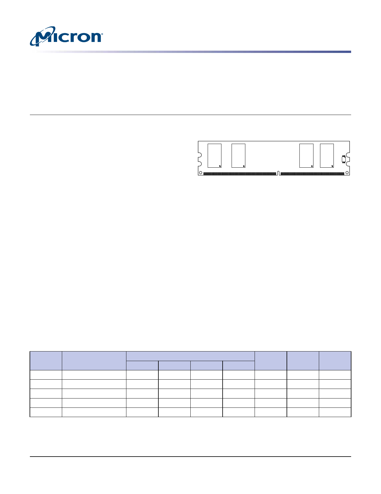
Figure 1: 240-Pin UDIMM (MO-237 R/C C)
Module height 30.0mm (1.18in)
Options
• Operating temperature
– Commercial (0°C ≤ TA ≤ +70°C)
– Industrial (–40°C ≤ TA ≤ +85°C)1
• Package
– 240-pin DIMM (lead-free)
• Frequency/CL2
– 2.5ns @ CL = 5 (DDR2-800)4
– 2.5ns @ CL = 6 (DDR2-800)4
– 3.0ns @ CL = 5 (DDR2-667)
– 3.75ns @ CL = 4 (DDR2-533)3
– 5.0ns @ CL = 3 (DDR2-400)3
Marking
None
I
Y
-80E
-800
-667
-53E
-40E
Notes:
1. Contact Micron for industrial temperature
module offerings.
2. CL = CAS (READ) latency.
3. Contact Micron for product availability.
4. Not available in 128MB and 256MB.
Table 1: Key Timing Parameters
Speed
Grade
-80E
-800
-667
-53E
-40E
Industry
Nomenclature
PC2-6400
PC2-6400
PC2-5300
PC2-4200
PC2-3200
CL = 6
800
800
–
–
–
Data Rate (MT/s)
CL = 5
CL = 4
800 533
667 533
667 553
– 553
– 400
CL = 3
400
400
400
400
400
tRCD
(ns)
12.5
15
15
15
15
tRP
(ns)
12.5
15
15
15
15
tRC
(ns)
55
55
55
55
55
PDF: 09005aef80ed6fda
htf4c16_32_64x64ay – Rev. H 3/10 EN
1 Micron Technology, Inc. reserves the right to change products or specifications without notice.
© 2003 Micron Technology, Inc. All rights reserved.
Products and specifications discussed herein are subject to change by Micron without notice.
1 page 
128MB, 256MB, 512MB (x64, SR) 240-Pin DDR2 SDRAM UDIMM
Pin Descriptions
Table 7: Pin Descriptions (Continued)
Symbol
SDA
RDQSx,
RDQS#x
Err_Out#
VDD/VDDQ
VDDSPD
VREF
VSS
NC
NF
NU
RFU
Type
I/O
Output
Output
(open drain)
Supply
Supply
Supply
Supply
–
–
–
–
Description
Serial data: Used to transfer addresses and data into and out of the SPD EEPROM on
the I2C bus.
Redundant data strobe (x8 devices only): RDQS is enabled/disabled via the LOAD
MODE command to the extended mode register (EMR). When RDQS is enabled, RDQS
is output with read data only and is ignored during write data. When RDQS is disa-
bled, RDQS becomes data mask (see DMx). RDQS# is only used when RDQS is enabled
and differential data strobe mode is enabled.
Parity error output: Parity error found on the command and address bus.
Power supply: 1.8V ±0.1V. The component VDD and VDDQ are connected to the mod-
ule VDD.
SPD EEPROM power supply: 1.7–3.6V.
Reference voltage: VDD/2.
Ground.
No connect: These pins are not connected on the module.
No function: These pins are connected within the module, but provide no functionality.
Not used: These pins are not used in specific module configurations/operations.
Reserved for future use.
PDF: 09005aef80ed6fda
htf4c16_32_64x64ay – Rev. H 3/10 EN
5 Micron Technology, Inc. reserves the right to change products or specifications without notice.
© 2003 Micron Technology, Inc. All rights reserved.
5 Page 
128MB, 256MB, 512MB (x64, SR) 240-Pin DDR2 SDRAM UDIMM
IDD Specifications
Table 10: DDR2 IDD Specifications and Conditions – 128MB (Continued)
Values shown for MT47H16M16 DDR2 SDRAM only and are computed from values specified in the 256Mb (16 Meg x 16)
component data sheet
Parameter
Symbol -667 -53E -40E Units
Operating bank interleave read current: All device banks interleaving
IDD7 1000 960 920 mA
reads; IOUT = 0mA; BL = 4, CL = CL (IDD), AL = tRCD (IDD) - 1 × tCK (IDD); tCK =
tCK (IDD), tRC = tRC (IDD), tRRD = tRRD (IDD), tRCD = tRCD (IDD); CKE is HIGH,
S# is HIGH between valid commands; Address bus inputs are stable during
deselects; Data bus inputs are switching
PDF: 09005aef80ed6fda
htf4c16_32_64x64ay – Rev. H 3/10 EN
11
Micron Technology, Inc. reserves the right to change products or specifications without notice.
© 2003 Micron Technology, Inc. All rights reserved.
11 Page | ||
| Páginas | Total 19 Páginas | |
| PDF Descargar | [ Datasheet MT4HTF3264AY.PDF ] | |
Hoja de datos destacado
| Número de pieza | Descripción | Fabricantes |
| MT4HTF3264AY | 256MB DDR2 SDRAM UDIMM | Micron |
| Número de pieza | Descripción | Fabricantes |
| SLA6805M | High Voltage 3 phase Motor Driver IC. |
Sanken |
| SDC1742 | 12- and 14-Bit Hybrid Synchro / Resolver-to-Digital Converters. |
Analog Devices |
|
DataSheet.es es una pagina web que funciona como un repositorio de manuales o hoja de datos de muchos de los productos más populares, |
| DataSheet.es | 2020 | Privacy Policy | Contacto | Buscar |